
 My Inquiry
 My Account


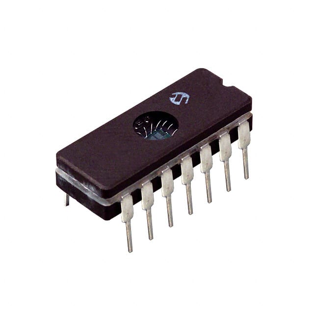
Microchip Technology TC9400EJD
- Part No.:
- TC9400EJD
- Manufacturer:
- Microchip Technology
- Category:
- V/F and F/V Converters
- Package:
- 14-CDIP (0.300", 7.62mm)
- Datasheet:
-
 TC9400EJD.pdf
- Description:
- IC F/V & V/F CONV 100KHZ 14CDIP
- Quantity:
- Payment:

- Shipping:

Inventory:2,457
Please send an inquiry. Send us your inquiry, and we will respond immediately.
Product details
Overview
TC9400EJD from Microchip Technology is a precision voltage-to-frequency (V/F) and frequency-to-voltage (F/V) converter IC designed for analog signal conditioning in data acquisition systems. It delivers 0.05% V/F linearity at 10 kHz, operates from ±4V to ±7.5V dual supply, supports DC–100 kHz F/V input range, and features programmable scale factor via external R/C components. It is used in tachometer circuits where analog motor speed signals are converted to digital-friendly pulse trains.
For engineers reviewing the TC9400EJD datasheet, TC9400EJD pinout, TC9400EJD application, or TC9400EJD equivalent, this page provides verified functional specifications, validated pin-level circuit roles, confirmed dual-mode (V/F + F/V) operation parameters, and real-world design constraints including bias current dependency, reference impedance sensitivity, and open-drain output interface requirements.
Technical Context
The TC9400EJD implements a charge-balancing architecture: in V/F mode, input current charges an integrator capacitor until threshold detection triggers a fixed-charge discharge via the VREFOUT pin, generating linearly proportional output pulses; in F/V mode, each input zero-crossing at the THRESHOLD DETECTOR pin dispenses identical charge packets into the integrator, producing a DC output voltage proportional to frequency. Its accuracy depends critically on external CREF and CINT stability and low-impedance VREF sourcing.
It uses low-power CMOS process technology enabling 27 mW typical dissipation and supports both dual-supply (±4V to ±7.5V) and single-supply (8V to 15V) configurations with level-shifting support. The device includes self-start circuitry to ensure reliable power-on initialization and features two open-drain outputs - PULSE FREQ OUT (frequency-proportional) and FREQ/2 OUT (symmetrical square wave) - sharing OUTPUT COMMON as source terminal.
Key Specifications
| Parameter | Value and Actual Design Meaning |
|---|---|
| V/F Linearity | 0.05% at 10 kHz full scale - defines maximum deviation from ideal transfer curve in voltage-to-pulse conversion |
| F/V Non-Linearity | 0.05% at 10–100 kHz - specifies worst-case error in frequency-to-DC voltage mapping over rated bandwidth |
| Supply Range | ±4V to ±7.5V dual supply - sets minimum/maximum rail voltages for stable internal biasing and output swing |
| Input Frequency Range (F/V) | 10 Hz to 100 kHz - usable input waveform frequency span before non-linearity exceeds spec limit |
| Gain Temp Drift | ±25 ppm/°C typical - quantifies how much full-scale gain shifts per degree Celsius, critical for wide-temp industrial use |
| Zero Offset | ±10 mV typical - baseline output error at zero input, adjustable via ZERO ADJ pin for system calibration |
| Power Dissipation | 27 mW typical - enables thermal management in dense PCB layouts without forced cooling |
Pinout & Package
TC9400EJD is housed in a 14-pin plastic DIP package (0.300" wide), RoHS-compliant, with through-hole mounting and standard JEDEC MO-001AC outline. Pin 13 is NC (no internal connection); all other pins have defined analog/digital functions as verified in DS21483D.
| Pin/Terminal | Circuit Role | Design Meaning |
|---|---|---|
| 1 IBIAS | Bias current setting node | Connects external 100 kΩ resistor to VSS to establish internal current reference; scaling affects max frequency and linearity trade-off |
| 2 ZERO ADJ | Integrator offset adjustment | Non-inverting op-amp input; used to null zero-input output error by trimming voltage at this pin |
| 3 IIN | V/F input current summing junction | Inverting op-amp input; accepts 10 µA full-scale current (up to 50 µA over-range); requires buffered voltage sources |
| 4 VSS | Negative supply rail | Reference for internal analog blocks; must be stable and low-noise; connects to RBIAS and VREF return path |
| 5 VREFOUT | Reference capacitor switching node | Internally toggles between VREF and integrator summing junction to inject fixed charge quanta (CREF × VREF) |
| 6 GND | Analog ground reference | Separate from OUTPUT COMMON; serves as reference for VREF, ZERO ADJ, and input circuitry to minimize noise coupling |
| 7 VREF | Reference voltage input | Accepts precision -5V (or low-impedance VSS); linearity degrades if source impedance exceeds 200 Ω |
| 8 PULSE FREQ OUT | Open-drain frequency output | Pulses LOW at rate proportional to input voltage; requires external pull-up; interfaces directly with TTL/CMOS logic |
| 9 OUTPUT COMMON | Source terminal for open-drain outputs | Shared drain-source return for both PULSE FREQ OUT and FREQ/2 OUT; connect to VSS or ground depending on logic level needs |
| 10 FREQ/2 OUT | Divided frequency output | Open-drain square wave at exactly half PULSE FREQ OUT frequency; transitions on rising edge of Pin 8 |
| 11 THRESHOLD DETECTOR | F/V input / V/F comparator input | Receives input waveform in F/V mode; in V/F mode, connected to AMP OUT to trigger reset pulses |
| 12 AMPLIFIER OUT | Integrator op-amp output | Provides negative-ramp waveform in V/F mode; delivers linear DC voltage in F/V mode; drives external filter networks |
| 13 NC | No internal connection | Not bonded; must remain unconnected to avoid parasitic coupling or mechanical stress |
| 14 VDD | Positive supply rail | Supplies internal logic and analog circuitry; decoupling capacitor required near pin for stability |
Key Features
| Feature | Design Value |
|---|---|
| Charge-balancing V/F architecture | Eliminates dependence on comparator threshold precision; linearity determined solely by CREF, VREF, and RIN stability |
| Dual-mode operation (V/F + F/V) | Single IC replaces separate converters; reconfigurable via external component topology without changing footprint |
| Self-start power-on circuitry | Guarantees reliable initialization even when integrator capacitor is pre-charged; prevents latch-up or undefined output state |
| Two synchronized open-drain outputs | PULSE FREQ OUT and FREQ/2 OUT share OUTPUT COMMON, enabling flexible timing capture (e.g., period vs. frequency measurement) |
| Low-impedance VREF requirement | Enables high-accuracy operation only when reference source impedance ≤200 Ω - guides selection of buffer op-amps or Zener networks |
Applications
| Tachometer Signal Conditioning | Microprocessor Data Acquisition Interface |
|---|---|
Use Scenario: Analog voltage from magnetic pickup sensor reflects rotating shaft speed in industrial motor control. IC Role / Device Role / Timing Role: TC9400EJD converts variable DC voltage into precise pulse train whose frequency is linearly proportional to RPM. Use Value: Enables direct counting by microcontroller timers without ADC sampling; eliminates quantization noise and improves resolution at low speeds. |
Use Scenario: Legacy analog sensors (e.g., pressure transducers) feed into embedded system lacking dedicated ADC channels. IC Role / Device Role / Timing Role: TC9400EJD acts as a low-cost, software-transparent analog front-end, transforming sensor voltage into countable frequency domain signal. Use Value: Leverages existing timer/counters in MCU for high-resolution measurement (13-bit effective) using simple firmware polling or interrupt-driven capture. |
| FM Demodulation Stage | Phase-Locked Loop Reference Generator |
Use Scenario: Recovering baseband audio from frequency-modulated carrier in communication receivers. IC Role / Device Role / Timing Role: TC9400EJD operates in F/V mode to convert instantaneous FM carrier frequency deviations into proportional analog voltage. Use Value: Provides monotonic, low-distortion demodulated output with 100 kHz bandwidth - sufficient for voice-grade signal recovery. |
Use Scenario: Generating stable, voltage-controlled oscillator (VCO) tuning voltage in analog PLL designs for clock synthesis. IC Role / Device Role / Timing Role: TC9400EJD serves as loop filter integrator and error-to-control-voltage converter in Type-II PLL architecture. Use Value: Delivers inherent integration function plus programmable gain via RINT/CINT, simplifying external compensation network. |
Equivalent & Alternatives
The following parts are listed as comparable options for similar voltage-to-frequency and frequency-to-voltage conversion applications.
| Alternative Part | Technical Difference | Application Difference | Selection Advice |
|---|---|---|---|
| TC9401EJD | 0.01% V/F linearity (vs. 0.05% for TC9400EJD); same pinout, package, and bias architecture | Required where higher linearity is mandated (e.g., metrology-grade instrumentation), accepting slightly higher cost | Select TC9401EJD only if system-level calibration budget cannot absorb 0.05% error; otherwise TC9400EJD offers optimal cost/performance balance. |
| LM331N/NOPB | Single-supply only (4–40V), 0.01% linearity, no F/V mode; different pinout and external component topology | Suitable for unipolar sensor interfaces but lacks dual-mode flexibility and ±supply operation of TC9400EJD | Choose LM331N/NOPB for cost-sensitive, single-rail designs where F/V functionality is unnecessary and layout space allows redesign. |
Compared with TC9401EJD, TC9400EJD trades 0.04% linearity for lower unit cost and identical integration effort; compared with LM331N/NOPB, TC9400EJD adds F/V capability, dual-supply support, and matched temperature drift specs - making it superior for bidirectional signal conditioning in industrial control.
Availability
TC9400EJD is available at Aetrix Electronics and suitable for tachometer systems, microprocessor-based data loggers, and analog telemetry interfaces requiring stable component supply across extended temperature ranges (-40°C to +85°C).
Supply support for TC9400EJD includes scheduled delivery planning, volume procurement assistance, BOM continuity management, traceable sourcing, and lifecycle availability coordination for OEM customers, industrial embedded developers, connected-device designers, and electronics production programs.
Manufacturer
Microchip Technology is a U.S.-based semiconductor manufacturer specializing in microcontrollers, analog devices, and interface ICs for industrial, automotive, and consumer applications.
The TC9400 family was designed specifically for high-accuracy analog signal conversion in resource-constrained embedded systems, emphasizing low power, external component minimization, and dual-mode operational flexibility.
FAQ
What is the maximum operating frequency of TC9400EJD in V/F mode?
The TC9400EJD supports up to 100 kHz full-scale output frequency in V/F mode under specified conditions (RBIAS = 100 kΩ, CREF = 27 pF, CINT = 75 pF). Exceeding 100 kHz requires reducing RBIAS to 20 kΩ, but this increases linearity error beyond the rated 0.05%. Pulse width remains ~3 µs across the range, limiting minimum duty cycle.
Can TC9400EJD operate from a single supply?
Yes, TC9400EJD supports single-supply operation from +8V to +15V using external biasing networks (e.g., Zener diodes) to generate internal virtual ground and reference levels. Figure 4-2 in DS21483D shows a validated +12V implementation. However, VREF must still be referenced to VSS (now a derived negative rail), and performance metrics like linearity assume proper decoupling and low-impedance references.
How does the TC9400EJD achieve 0.05% V/F linearity?
The TC9400EJD achieves 0.05% V/F linearity through its charge-balancing architecture: each output pulse corresponds to removal of a fixed charge (CREF × VREF) from the integrator capacitor. Since linearity depends only on capacitor matching and reference voltage stability-not comparator thresholds or pulse timing-external component selection (low-drift CREF, metal-film RIN, low-Z VREF) directly determines achievable accuracy.
What is the role of the OUTPUT COMMON pin on TC9400EJD?
The OUTPUT COMMON pin (Pin 9) serves as the shared source terminal for both open-drain outputs - PULSE FREQ OUT (Pin 8) and FREQ/2 OUT (Pin 10). It must be connected to either VSS (for negative-swing logic) or ground (for standard TTL/CMOS pull-up), defining the low-state voltage level. Separating OUTPUT COMMON from GND (Pin 6) prevents ground-loop interference in mixed-signal layouts.
Does TC9400EJD require external passive components to function?
Yes, TC9400EJD requires at minimum three resistors (RBIAS, RIN, RINT) and two capacitors (CREF, CINT) to configure V/F or F/V operation. These set full-scale range, zero point, ripple rejection, and response time. The device datasheet provides exact equations (e.g., FOUT = VIN / (RIN × CREF × VREF)) and recommended values for 1 kHz, 10 kHz, and 100 kHz scales - omitting any one component prevents functional operation.
TC9400EJD Specifications
- Product attributes
- Attribute value
- Manufacturer:
- Microchip Technology
- Series:
- -
- Package/Case:
- 14-CDIP (0.300", 7.62mm)
- Packaging:
- Tube
- Product Status:
- Obsolete
- Type:
- Volt to Frequency and Frequency to Volt
- Frequency - Max:
- 100 kHz
- Full Scale:
- ±40ppm/°C
- Linearity:
- ±0.05%
- Mounting Type:
- Through Hole
- Grade:
- -
- Qualification:
- -
- Supplier Device Package:
- 14-CERDIP
TC9400EJD FAQ
1.How can I place an order for TC9400EJD through Aetrix?
Please submit a Request for Quotation (RFQ) for TC9400EJD on Aetrix. Our sales agent will provide a competitive quotation and guide you through the order confirmation once you accept the terms.
2.Are the price and stock information for TC9400EJD reliable?
The price and inventory of TC9400EJD are updated periodically and may fluctuate due to market conditions. Stock and pricing data are typically refreshed every 24 hours. Quotation validity for TC9400EJD is usually 5 days.
3.What payment methods are accepted for TC9400EJD?
We accept Wire Transfer, PayPal, Credit Card, Western Union, MoneyGram, and Escrow for TC9400EJD transactions.
Note: Certain payment methods may incur a processing fee.
4.How is shipping managed for TC9400EJD?
TC9400EJD orders can be shipped via leading logistics carriers, including DHL, UPS, FedEx, TNT, or Registered Mail.
Once your TC9400EJD order is processed, you will receive an email with the shipment details and tracking number.
Note: Tracking information may take up to 24 hours to appear. Express delivery typically takes 3–5 business days.
5.How can I obtain technical support or documentation for TC9400EJD?
For technical support, including TC9400EJD datasheets, pinout diagrams, or application guidance, please contact our engineering support team. They can provide detailed documentation and assistance for your TC9400EJD requirements.
6.How does Aetrix verify that TC9400EJD is sourced from the original manufacturer or authorized distributors?
All TC9400EJD products on Aetrix are procured from qualified distributors and authorized channels. Our dedicated quality assurance team conducts strict verification, including traceability checks and, if necessary, third-party testing. This ensures that TC9400EJD meets industry standards.
7.What is the process for return or replacement of TC9400EJD?
All TC9400EJD units undergo pre-shipment inspection (PSI). If there is an issue with TC9400EJD, returns or replacements are accepted under the following conditions:
1.Quantity discrepancies, incorrect items, or visible external defects (such as breakage or corrosion), acknowledged by Aetrix.
2.The issue is reported within 90 days of delivery.
3.The TC9400EJD part is unused and in its original packaging.
Return procedure for TC9400EJD:
1.Submit a request within 90 days.
2.Obtain a Return Material Authorization (RMA) from Aetrix.
TC9400EJD Tags

-
LM2907MX-8/NOPB
Texas Instruments

-
LM2907N/NOPB
Texas Instruments

-
LM2907N-8/NOPB
Texas Instruments
-
LM331N/NOPB
Texas Instruments
-
AD7740YRMZ
Analog Devices Inc.
-
AD7740YRTZ-REEL7
Analog Devices Inc.
-
LM231N/NOPB
Texas Instruments
-
AD7741BRZ-REEL7
Analog Devices Inc.
-
VFC32KP
Texas Instruments

-
VFC32KU
Texas Instruments
-
AD654JRZ-REEL
Analog Devices Inc.
-
AD654JRZ
Analog Devices Inc.
Tech Hub

TTL and CMOS logic families differ in thresholds, loading, output drive, power and timing. This engineering guide compares 74HC and 74HCT, calculates noise margins and checks 3.3 V/5 V compatibility.

A practical engineering guide to 3.3V and 5V logic compatibility, input thresholds, resistor dividers, translator ICs, MOSFET level shifting, I2C pull-ups, timing limits and power-sequencing risks.

The 74HC595 uses push-pull logic outputs, while the TPIC6B595 uses 50 V open-drain DMOS sinks for higher-power loads. This guide compares timing, current limits, 3.3 V interfacing, load wiring, thermal…

The 74HC595 converts serial data into eight stable parallel outputs. This guide covers pin functions, shift and storage timing, OE and MR behavior, drive-current limits, cascading, voltage compatibilit…

A technical comparison of level-sensitive latches and edge-triggered flip-flops, covering timing windows, setup and hold limits, master–slave operation, time borrowing, race-through, HDL inference and…

A D latch stores one bit while Enable controls when data can pass. This reference covers gate-level operation, truth tables, transparency, setup and hold timing, LE versus OE, common ICs and practical …

An SR latch stores one bit through cross-coupled feedback. This engineering reference covers NOR and NAND implementations, truth tables, forbidden-state recovery, gated operation, switch debouncing, fa…

Latch circuits retain one bit through feedback. This technical reference covers SR and D latches, truth tables, transparency, timing limits, latch-versus-flip-flop behavior, applications and common log…

An engineering guide to LED driver operation, constant-current and constant-voltage outputs, linear and switching topologies, dimming, IC selection, calculations, replacement compatibility, and fault c…

Operational amplifier guide covering op amp basics, feedback, ideal vs real op amps, common configurations, buffer circuits, offset, bias current, gain-bandwidth, slew rate, rail-to-rail limits and sel…


