
 My Inquiry
 My Account


Toshiba Semiconductor and Storage TCKE812NL,RF
- Part No.:
- TCKE812NL,RF
- Manufacturer:
- Toshiba Semiconductor and Storage
- Category:
- Current Regulation/Management
- Package:
- 10-WFDFN Exposed Pad
- Datasheet:
-
 TCKE812NL,RF.pdf
- Description:
- IC ELECTRONIC FUSE 10WSON
- Quantity:
- Payment:

- Shipping:

Inventory:52,356
Please send an inquiry. Send us your inquiry, and we will respond immediately.
Product details
Overview
TCKE812NL,RF from Toshiba Electronic Devices & Storage Corporation is a 18 V, 5 A latched eFuse IC with reverse current blocking control, adjustable overcurrent protection (up to 5.0 A), and 15.1 V (typ.) overvoltage clamp. It integrates internal MOSFET switching, thermal shutdown, UVLO, and slew-rate control via external capacitor - designed for high-reliability power rail protection in 12 V systems such as HDD power supplies and battery charging circuits.
For engineers reviewing the TCKE812NL,RF datasheet, TCKE812NL,RF pinout, TCKE812NL,RF application, or TCKE812NL,RF equivalent, this page delivers verified electrical parameters, WSON10B package mapping, real-world protection timing behavior (e.g., 150 ns fast-trip response), latch-mode fault handling, and precise RILIM/CdV/dT design guidance for stable 12 V rail deployment.
Technical Context
The TCKE812NL,RF implements a single-input/single-output eFuse architecture with integrated N-channel power MOSFET and dedicated EFET gate driver for external reverse-blocking FET control. Its protection logic combines adjustable current limiting (via ILIM resistor), fixed 15.1 V overvoltage clamp, and thermal shutdown at 160°C with 20°C hysteresis.
It operates across −40°C to +85°C ambient, supports VIN from 4.4 V to 18.0 V, and uses EN/UVLO pin for dual-function enable control and programmable under-voltage lockout. Fault response is latched - requiring external reset via EN/UVLO low-to-high transition after fault clearance.
Key Specifications
| Parameter | Value and Actual Design Meaning |
|---|---|
| Max Input Voltage | 18.0 V - supports direct connection to 12 V automotive or industrial rails with margin for transients |
| Continuous Output Current | 5.0 A - enables use in high-current power distribution nodes without external current-sense amplifiers |
| ON Resistance | 28 mΩ (typ.) - minimizes conduction loss (≤140 mW at 5 A) and self-heating during sustained load |
| Overvoltage Clamp | 15.1 V (typ.) - protects downstream 12 V logic and analog circuitry from input surges exceeding rail rating |
| Fault Response Mode | Latched - holds output off until explicit EN/UVLO reset, preventing uncontrolled auto-retry in persistent faults |
| Fast-Trip Delay | 150 ns (typ.) - detects and disables output within one nanosecond-scale cycle of hard short (≤10 mΩ) |
| Thermal Shutdown Threshold | 160°C junction - activates before silicon degradation, with 20°C hysteresis enabling safe cooldown before recovery |
Pinout & Package
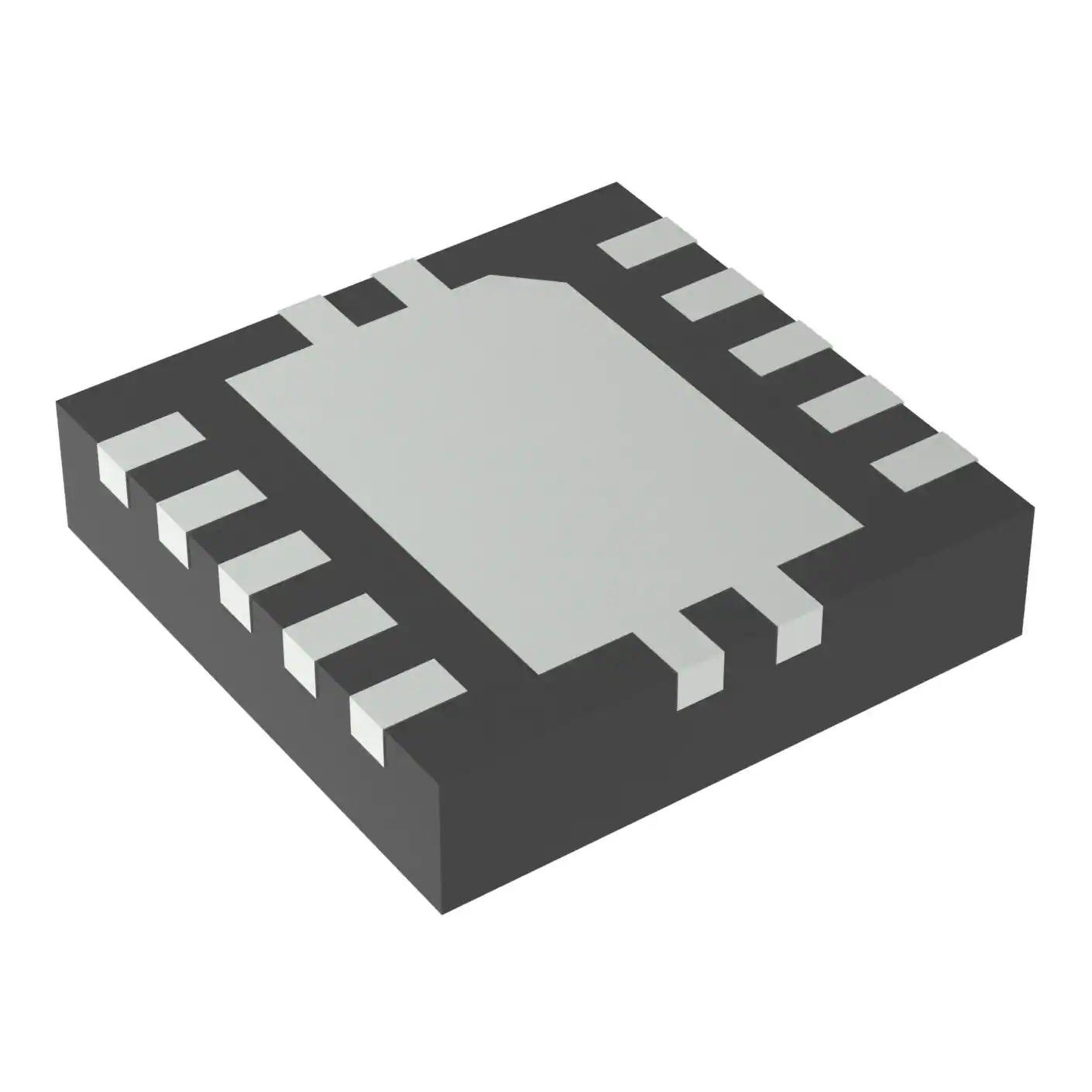
Package: WSON10B (3.0 mm × 3.0 mm, 0.7 mm height, 0.5 mm pitch, exposed thermal pad). Compact footprint suitable for space-constrained portable and embedded power modules.
| Pin/Terminal | Circuit Role | Design Meaning |
|---|---|---|
| dV/dT | Slew rate control input | Connects external capacitor (1–100 nF) to set VOUT ramp time from 300 μs to 4.8 ms - prevents inrush-induced OCP false triggers |
| EN/UVLO | Enable & UVLO threshold input | Dual-function pin: enables output when >1.1 V (typ.), disables below 0.96 V (typ.); configurable UVLO trip via external resistor divider |
| VIN | Main power input | Supplies internal circuitry and powers internal MOSFET switch; accepts 4.4–18.0 V with transient tolerance |
| GND | Power and signal reference | Common return path for all currents; requires low-impedance PCB plane for thermal and noise performance |
| ILIM | Current limit set input | Resistor to GND sets OCP threshold from 0.5 A to 5.15 A (e.g., 20 kΩ = 5.15 A typ. at VIN−VOUT = 1 V) |
| EFET | External FET gate driver | Drives N-ch MOSFET gate to block reverse current; outputs boosted voltage (VIN+4.9 V typ.) for full enhancement |
| VOUT | Protected power output | Delivers regulated, clamped, and current-limited output; three pins (6,7,8) paralleled for low-inductance, high-current routing |
Key Features
| Feature | Design Value |
|---|---|
| Reverse current blocking support | Built-in EFET driver enables external N-ch MOSFET to prevent backflow during VIN removal or shutdown - critical for bidirectional power domains |
| Programmable slew rate control | External CdV/dT capacitor adjusts VOUT rise time from 300 μs to 4.8 ms - eliminates inrush-induced false OCP trips and output overshoot |
| Latched fault response | Output remains disabled after overcurrent, overvoltage, or thermal fault until EN/UVLO is cycled - ensures deterministic system-level fault containment |
| IEC62368-1 certified | Meets end-equipment safety standard for audio/video, IT and communication technology equipment - reduces certification burden for final products |
| Adjustable UVLO threshold | External resistor divider on EN/UVLO pin sets custom under-voltage turn-on point above 4.15 V - enables staged power-up sequencing |
Applications
| Hard Disk Drive Power Supply | Battery Charging Circuit Protection |
|---|---|
Use Scenario: Protecting 12 V motor and controller supply in enterprise HDD enclosures against short circuits, inrush, and input transients. IC Role / Device Role / Timing Role: Primary power switch and fault manager; provides 150 ns fast-trip response and latched disable to prevent repeated stress during mechanical failure. Use Value: Eliminates need for discrete fuses and relays while maintaining IEC62368-1 compliance and enabling automated fault logging via EN/UVLO status monitoring. | Use Scenario: Securing the output stage of a 12 V Li-ion battery charger where load disconnection must prevent reverse discharge into failed cells. IC Role / Device Role / Timing Role: Bidirectional protection element; EFET-driven external MOSFET blocks reverse current when charger is powered down, while 15.1 V OVC clamps surge from hot-plug events. Use Value: Enables safe hot-swap capability and extends battery pack life by eliminating parasitic drain paths during standby or fault conditions. |
| Industrial PLC I/O Module | Automotive Body Control Module (BCM) |
Use Scenario: Distributing 12 V power to isolated digital I/O channels in programmable logic controllers subject to ESD and cable fault events. IC Role / Device Role / Timing Role: Per-channel eFuse with independent RILIM tuning; latched mode prevents spurious resets during transient ESD-induced overcurrent. Use Value: Provides channel-level diagnostics and isolation without software intervention - simplifies firmware and improves MTBF in harsh factory environments. | Use Scenario: Protecting 12 V accessory rails (e.g., lighting, window motors) in BCMs where load dumps and jump-start surges exceed 24 V. IC Role / Device Role / Timing Role: Front-end protection IC; 18 V absolute max rating and 15.1 V OVC withstand 24 V load-dump spikes while limiting energy delivered to downstream loads. Use Value: Replaces TVS-diode + fuse combinations with single-component solution that maintains functional safety integrity per ISO 26262 ASIL-B requirements. |
Equivalent & Alternatives
The following parts are listed as comparable options for similar eFuse protection applications.
| Alternative Part | Technical Difference | Application Difference | Selection Advice |
|---|---|---|---|
| TCKE812NA,RF | Auto-retry fault response vs. latched; identical OVC (15.1 V), RON (28 mΩ), and VIN range | Suitable for non-critical loads where automatic recovery is acceptable after transient fault clears | Select TCKE812NA,RF only if system firmware can monitor retry cycles and log persistent faults |
| TPS259472LVR | TI device with 18 V max, 5.5 A, 22 mΩ RON, but fixed 14.5 V OVC and no EFET driver for reverse blocking | Lacks integrated reverse-current blocking - requires external circuitry for backflow prevention | Choose only if reverse blocking is unnecessary and tighter RON tolerance (±15%) is prioritized over EFET control |
Compared with TCKE812NA,RF, the TCKE812NL,RF provides deterministic fault containment via latching, while versus TPS259472LVR it delivers unique EFET-driven reverse blocking - making it the sole option among these three for applications requiring both latch-mode safety and bidirectional current control.
Availability
TCKE812NL,RF is available at Aetrix Electronics and suitable for hard disk drive power supplies, battery charging circuits, industrial PLC I/O modules, and automotive body control modules requiring stable component supply, long-term lifecycle support, and IEC62368-1 certified protection.
Supply support for TCKE812NL,RF includes scheduled delivery planning, volume procurement assistance, BOM continuity management, traceable sourcing, and lifecycle availability coordination for OEM customers, industrial embedded developers, connected-device designers, and electronics production programs.
Manufacturer
Toshiba Electronic Devices & Storage Corporation designs high-reliability semiconductor solutions for power management, motor control, and interface applications, with emphasis on industrial and computing markets.
The TCKE8xx series was developed specifically for robust, programmable eFuse protection in 12 V and 5 V power distribution networks - targeting applications where fuse replacement is impractical and system-level fault containment is mandatory.
FAQ
What is the overvoltage clamp voltage of the TCKE812NL,RF?
The TCKE812NL,RF features a fixed overvoltage clamp of 15.1 V (typical), with a guaranteed range of 14.11 V to 16.14 V across −40°C to +85°C ambient. This value applies specifically to the TCKE812 variant and is confirmed in Section 11.3 of the official Toshiba datasheet. The TCKE812NL,RF uses this clamp to protect downstream 12 V circuitry from input surges without requiring external components.
How does the latched fault response of the TCKE812NL,RF differ from auto-retry types?
The TCKE812NL,RF enters a latched-off state upon overcurrent, overvoltage, or thermal fault and remains disabled until the EN/UVLO pin is actively cycled from low to high. Unlike auto-retry variants (e.g., TCKE812NA,RF), it does not attempt autonomous recovery. This behavior ensures fault persistence is visible to system firmware and prevents uncontrolled re-energization in hazardous conditions - a key requirement in industrial and automotive safety-critical designs using the TCKE812NL,RF.
Can the TCKE812NL,RF be used without an external MOSFET for reverse current blocking?
Yes, the TCKE812NL,RF functions fully as a standalone eFuse without an external MOSFET. The EFET pin may be left floating if reverse current blocking is not required. When unused, the internal circuitry ignores the EFET driver output, and the device operates normally with forward-only current flow. Reverse blocking is an optional feature enabled only when an N-channel MOSFET is connected to the EFET pin - no penalty in cost, layout, or performance occurs when omitting it for unidirectional applications using the TCKE812NL,RF.
What is the recommended external capacitor value for dV/dT control on the TCKE812NL,RF?
Toshiba specifies CdV/dT values from 1 nF (typ.) to 100 nF (max) for the TCKE812NL,RF. A 1 nF capacitor yields ~4.8 ms typical VOUT ramp time at 12 V input, while open-circuit (no capacitor) gives ~500 μs. Designers select based on load capacitance and inrush sensitivity: 1–10 nF is typical for HDD or battery-charger outputs with ≥100 μF bulk capacitance. The exact value must be validated on the target PCB due to parasitic effects - the TCKE812NL,RF's dV/dT pin tolerates up to 6.0 V and draws only 250 nA.
Does the TCKE812NL,RF require a heatsink in 5 A continuous operation?
No external heatsink is required for the TCKE812NL,RF at 5 A DC in typical applications. With 28 mΩ (typ.) RON, conduction loss is ~700 mW, and the WSON10B package (θJA ≈ 52°C/W on 4-layer FR4) results in ~36°C junction rise above ambient. At 85°C max ambient, junction temperature stays well below the 160°C thermal shutdown threshold. However, board-level copper area under the exposed thermal pad must be ≥100 mm² and connected via ≥4 thermal vias to inner ground planes - this thermal design is mandatory to achieve rated performance with the TCKE812NL,RF.
TCKE812NL,RF Specifications
- Product attributes
- Attribute value
- Manufacturer:
- Toshiba Semiconductor and Storage
- Series:
- -
- Package/Case:
- 10-WFDFN Exposed Pad
- Packaging:
- Tape & Reel (TR)
- Product Status:
- Active
- Function:
- Electronic Fuse
- Sensing Method:
- -
- Accuracy:
- -
- Voltage - Input:
- 4.4V ~ 18V
- Current - Output:
- 5A
- Operating Temperature:
- -40°C ~ 85°C
- Grade:
- -
- Qualification:
- -
- Mounting Type:
- Surface Mount
- Supplier Device Package:
- 10-WSONB (3x3)
TCKE812NL,RF FAQ
1.How can I place an order for TCKE812NL,RF through Aetrix?
Please submit a Request for Quotation (RFQ) for TCKE812NL,RF on Aetrix. Our sales agent will provide a competitive quotation and guide you through the order confirmation once you accept the terms.
2.Are the price and stock information for TCKE812NL,RF reliable?
The price and inventory of TCKE812NL,RF are updated periodically and may fluctuate due to market conditions. Stock and pricing data are typically refreshed every 24 hours. Quotation validity for TCKE812NL,RF is usually 5 days.
3.What payment methods are accepted for TCKE812NL,RF?
We accept Wire Transfer, PayPal, Credit Card, Western Union, MoneyGram, and Escrow for TCKE812NL,RF transactions.
Note: Certain payment methods may incur a processing fee.
4.How is shipping managed for TCKE812NL,RF?
TCKE812NL,RF orders can be shipped via leading logistics carriers, including DHL, UPS, FedEx, TNT, or Registered Mail.
Once your TCKE812NL,RF order is processed, you will receive an email with the shipment details and tracking number.
Note: Tracking information may take up to 24 hours to appear. Express delivery typically takes 3–5 business days.
5.How can I obtain technical support or documentation for TCKE812NL,RF?
For technical support, including TCKE812NL,RF datasheets, pinout diagrams, or application guidance, please contact our engineering support team. They can provide detailed documentation and assistance for your TCKE812NL,RF requirements.
6.How does Aetrix verify that TCKE812NL,RF is sourced from the original manufacturer or authorized distributors?
All TCKE812NL,RF products on Aetrix are procured from qualified distributors and authorized channels. Our dedicated quality assurance team conducts strict verification, including traceability checks and, if necessary, third-party testing. This ensures that TCKE812NL,RF meets industry standards.
7.What is the process for return or replacement of TCKE812NL,RF?
All TCKE812NL,RF units undergo pre-shipment inspection (PSI). If there is an issue with TCKE812NL,RF, returns or replacements are accepted under the following conditions:
1.Quantity discrepancies, incorrect items, or visible external defects (such as breakage or corrosion), acknowledged by Aetrix.
2.The issue is reported within 90 days of delivery.
3.The TCKE812NL,RF part is unused and in its original packaging.
Return procedure for TCKE812NL,RF:
1.Submit a request within 90 days.
2.Obtain a Return Material Authorization (RMA) from Aetrix.
TCKE812NL,RF Tags
.jpg)
-
PSSI2021SAY,115
Nexperia USA Inc.

-
BCR401RE6327HTSA1
Infineon Technologies

-
INA199B2DCKR
Texas Instruments
-
INA199A1DCKR
Texas Instruments
-
INA199B1DCKR
Texas Instruments
-
NSI45015WT1G
onsemi
-
NSI45020T1G
onsemi
-
NSI45030AT1G
onsemi
-
NSI45025AT1G
onsemi
-
NSI45020AT1G
onsemi
-
NSI50010YT1G
onsemi
-
LM334Z/NOPB
Texas Instruments
Tech Hub

Counterfeit components can hide behind convincing markings and passing basic function tests. This engineering reference covers source traceability, external inspection, X-ray, XRF, electrical testing, …

A practical engineering and sourcing framework covering lifecycle verification, lifetime-buy calculations, replacement qualification, supplier checks and counterfeit-risk controls.

TTL and CMOS logic families differ in thresholds, loading, output drive, power and timing. This engineering guide compares 74HC and 74HCT, calculates noise margins and checks 3.3 V/5 V compatibility.

A practical engineering guide to 3.3V and 5V logic compatibility, input thresholds, resistor dividers, translator ICs, MOSFET level shifting, I2C pull-ups, timing limits and power-sequencing risks.

The 74HC595 uses push-pull logic outputs, while the TPIC6B595 uses 50 V open-drain DMOS sinks for higher-power loads. This guide compares timing, current limits, 3.3 V interfacing, load wiring, thermal…

The 74HC595 converts serial data into eight stable parallel outputs. This guide covers pin functions, shift and storage timing, OE and MR behavior, drive-current limits, cascading, voltage compatibilit…

A technical comparison of level-sensitive latches and edge-triggered flip-flops, covering timing windows, setup and hold limits, master–slave operation, time borrowing, race-through, HDL inference and…

A D latch stores one bit while Enable controls when data can pass. This reference covers gate-level operation, truth tables, transparency, setup and hold timing, LE versus OE, common ICs and practical …

An SR latch stores one bit through cross-coupled feedback. This engineering reference covers NOR and NAND implementations, truth tables, forbidden-state recovery, gated operation, switch debouncing, fa…

Latch circuits retain one bit through feedback. This technical reference covers SR and D latches, truth tables, transparency, timing limits, latch-versus-flip-flop behavior, applications and common log…


