Send an Inquiry

To receive a quote for your project, please fill in the following information, and we’ll get back to you promptly.

Name*
Company*
Email Address*
Phone/WhatsApp
Part Number*
Quantity*
Message
Submit Inventory List

Please fill in the following information, and we’ll get back to you promptly.

Name*
Company*
Email Address*
Phone/WhatsApp
Upload My List
Message

Toshiba Semiconductor and Storage TCR2EF30,LM(CT
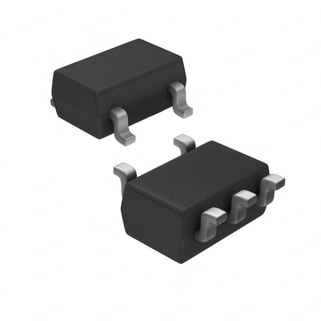
Part No.:
TCR2EF30,LM(CT
Manufacturer:
Toshiba Semiconductor and Storage
Category:
Voltage Regulators - Linear, Low Drop Out (LDO) Regulators
Package:
SC-74A, SOT-753
Datasheet:
AetrixTCR2EF30,LM(CT.pdf
Description:
IC REG LINEAR 3V 200MA SMV
Quantity:
Payment:
Payment
Shipping:
Shipping

Inventory:294

Please send an inquiry. Send us your inquiry, and we will respond immediately.

Part Number
Quantity*
Price
Name*
Company
Email*
Comments

Product details

Overview

TCR2EF30,LM(CT) from Toshiba Electronic Devices & Storage Corporation is a 3.0 V fixed-output CMOS low dropout (LDO) regulator delivering up to 200 mA with 150 mV typical dropout voltage at 150 mA load, 35 μVrms output noise, and ±60 mV load transient response - designed for powering sensitive analog and RF circuitry in portable and space-constrained systems.

For engineers reviewing the TCR2EF30,LM(CT) datasheet, TCR2EF30,LM(CT) pinout, TCR2EF30,LM(CT) application, or TCR2EF30,LM(CT) equivalent, key selection criteria include its fast transient performance under 1–150 mA step loads, ±1.0% output accuracy (≥1.8 V), 35 μVrms noise floor, ceramic capacitor compatibility (CIN = 0.1 μF, COUT = 1.0 μF), and on/off control interface with auto-discharge function.

Technical Context

The TCR2EF30,LM(CT) implements a CMOS-based LDO architecture with integrated overcurrent protection and an active pull-down on the CONTROL pin to ensure rapid discharge of output capacitance during shutdown. Its internal reference and error amplifier are optimized for stability with low-ESR ceramic capacitors.

It operates across −40°C to +85°C ambient temperature, supports input voltages from 1.5 V to 5.5 V, and maintains regulation down to VIN = VOUT + 0.5 V (i.e., as low as 3.5 V input for 3.0 V output). The device achieves 73 dB ripple rejection at 1 kHz and exhibits only 100 ppm/°C output voltage drift over temperature.

Key Specifications

Parameter Value and Actual Design Meaning
Output Voltage Fixed 3.0 V ±1.0% (guaranteed for 1.8 V ≤ VOUT)
Max Output Current 200 mA DC - sufficient for powering RF transceivers, ADCs, and low-power microcontrollers
Dropout Voltage 150 mV typ. at IOUT = 150 mA - enables operation from 3.15 V input while maintaining 3.0 V output
Output Noise 35 μVrms (10 Hz–100 kHz) - preserves signal integrity in precision analog and RF front-ends
Load Transient Response ±60 mV deviation for 1 mA ⇔ 150 mA load steps with 1.0 μF COUT - minimizes supply-induced jitter
Quiescent Current 35 μA typ. at zero load - extends battery life in always-on sensor nodes
Ripple Rejection 73 dB typ. at 1 kHz - suppresses switching noise from upstream DC/DC converters

Pinout & Package

TCR2EF30,LM(CT) is packaged in the ESV (SOT-553) footprint: ultra-small 1.6 mm × 1.6 mm × 0.55 mm, 5-pin surface-mount package with exposed pad not connected internally. Weight is 3.0 mg (typ.).

Pin/Terminal Circuit Role Design Meaning
VIN Input power supply connection Accepts 1.5–5.5 V; requires ≥0.1 μF ceramic bypass capacitor close to pin
VOUT Regulated output voltage node Delivers stable 3.0 V; requires ≥1.0 μF ceramic output capacitor with ESR <10 Ω
GND Power ground reference Common return path for input, output, and control circuits; must be low-impedance
CONTROL Enable/disable logic input Active-high: ≥1.0 V turns regulator ON; ≤0.4 V forces shutdown and activates auto-discharge
NC No-connect terminal Internally unconnected; must remain floating or grounded per layout best practices

Key Features

Feature Design Value
Fast Load Transient Response ±60 mV output deviation for 1 mA ↔ 150 mA load steps - reduces need for oversized bulk capacitance
Auto-Discharge Function Internal discharge path activates when CONTROL = LOW - prevents residual voltage hold-up on VOUT
Ceramic Capacitor Compatibility Stable with CIN ≥ 0.1 μF and COUT ≥ 1.0 μF ceramic types - eliminates need for tantalum or electrolytic caps
Low Quiescent Current 35 μA typ. at zero load - enables >1-year battery life in 10 μA average-current IoT endpoints
High Accuracy Output ±1.0% tolerance over temperature and line/load - avoids post-regulation trimming in precision systems

Applications

RF Front-End Power Portable Sensor Node Supply

Use Scenario: Powering 2.4 GHz BLE transceiver ICs and low-noise amplifiers in compact wearables.

IC Role / Device Role / Timing Role: Primary 3.0 V bias rail with ultra-low noise and fast transient recovery to prevent TX/RX desense.

Use Value: 35 μVrms noise and ±60 mV transient swing preserve EVM and sensitivity specs without added filtering.

Use Scenario: Supplying MEMS accelerometers and 16-bit SAR ADCs in battery-powered condition monitoring devices.

IC Role / Device Role / Timing Role: Precision analog domain regulator enabling <1 LSB INL error and stable reference coupling.

Use Value: ±1.0% output accuracy and 100 ppm/°C drift eliminate calibration overhead across industrial temperature range.

Always-On Microcontroller Core Low-Power Display Backlight Bias

Use Scenario: Providing standby voltage to ARM Cortex-M0+ MCU cores during deep-sleep modes.

IC Role / Device Role / Timing Role: Always-active LDO with CONTROL pin synchronized to system wake/sleep states.

Use Value: 35 μA quiescent current and auto-discharge reduce leakage-induced battery drain by >95% vs. non-shutdown regulators.

Use Scenario: Biasing white LED strings in smart thermostats and handheld HMI displays.

IC Role / Device Role / Timing Role: Constant-voltage source with fast turn-on/turn-off to support PWM dimming control.

Use Value: 150 mV dropout enables use of single-cell Li-ion (3.0–4.2 V) without intermediate buck conversion loss.

Equivalent & Alternatives

The following parts are listed as comparable options for similar LDO regulator applications.

Alternative Part Technical Difference Application Difference Selection Advice
TCS2EF30,LM(CT) Same pinout, identical electrical specs, but uses SMV (SOT-25) package (2.8 mm × 2.9 mm) instead of ESV Preferred where board real estate allows larger footprint and thermal mass improves power dissipation margin Select when PCB layout constraints permit SOT-25 and higher board-mounted PD rating (580 mW vs. 320 mW) is needed
XC6206P302MR-G 3.0 V fixed LDO; 150 mA max; 250 mV dropout; 40 μVrms noise; no auto-discharge; SOT-25 package Lacks CONTROL pin functionality and fast discharge - unsuitable for systems requiring clean power sequencing Consider only for cost-sensitive, non-sequenced applications where 250 mV dropout and absence of auto-discharge are acceptable

Compared with TCR2EF30,LM(CT), the TCS2EF30,LM(CT) offers identical regulation performance in a thermally robust SOT-25 package, while the XC6206P302MR-G trades control flexibility and transient speed for lower unit cost - making TCR2EF30,LM(CT) optimal for space-constrained, sequenced, and noise-sensitive designs.

Availability

TCR2EF30,LM(CT) is available at Aetrix Electronics and suitable for RF front-end power, portable sensor node supply, and always-on microcontroller core applications requiring stable component supply, long-term lifecycle assurance, and RoHS-compliant packaging.

Supply support for TCR2EF30,LM(CT) includes scheduled delivery planning, volume procurement assistance, BOM continuity management, traceable sourcing, and lifecycle availability coordination for OEM customers, industrial embedded developers, connected-device designers, and electronics production programs.

Manufacturer

Toshiba Electronic Devices & Storage Corporation designs high-reliability semiconductor solutions for industrial, automotive, and consumer electronics, with emphasis on energy efficiency and miniaturization.

The TCR2EF series targets ultra-compact, low-noise power management in portable and wireless systems - specifically engineered for analog/RF signal chains where dropout, noise, and transient response directly impact system-level performance.

FAQ

What is the maximum input voltage rating for TCR2EF30,LM(CT)?

The absolute maximum input voltage for TCR2EF30,LM(CT) is 6.0 V. However, the recommended operating input voltage range is 1.5 V to 5.5 V. Exceeding 5.5 V may trigger overvoltage stress even if within absolute maximum ratings, and sustained operation above this range risks reliability degradation per Toshiba's derating guidelines.

Does TCR2EF30,LM(CT) require external components to operate stably?

Yes - TCR2EF30,LM(CT) requires a minimum 0.1 μF ceramic capacitor on VIN and a minimum 1.0 μF ceramic capacitor on VOUT, both placed as close as possible to their respective pins. Toshiba specifies ESR <10 Ω for the output capacitor; no additional compensation network or feedforward capacitor is needed due to internal stability optimization.

How does the CONTROL pin function on TCR2EF30,LM(CT)?

The CONTROL pin on TCR2EF30,LM(CT) is an active-high enable input: applying ≥1.0 V (up to 5.5 V) turns the regulator ON; applying ≤0.4 V forces shutdown and activates the internal auto-discharge path to rapidly deplete VOUT capacitance. An open or floating CONTROL pin defaults to OFF state due to internal pull-down.

What is the thermal performance difference between ESV and SMV packages for TCR2EF30,LM(CT)?

TCR2EF30,LM(CT) in ESV (SOT-553) has a board-mounted power dissipation rating of 320 mW on a 30 mm × 30 mm × 0.8 mm FR4 board, while the SMV (SOT-25) variant supports 580 mW on a 25.4 mm × 25.4 mm × 1.6 mm FR4 board. The ESV's smaller size sacrifices ~45% thermal margin but enables 60% footprint reduction - critical for ultra-dense layouts.

Is TCR2EF30,LM(CT) suitable for automotive applications?

TCR2EF30,LM(CT) is specified for −40°C to +85°C operating temperature and meets industrial-grade reliability standards, but it is not AEC-Q200 qualified. It is suitable for under-dash infotainment peripherals or cabin sensors where full automotive qualification is not mandated; for safety-critical or engine-bay applications, Toshiba's automotive-qualified TAxx series should be used instead.

TCR2EF30,LM(CT Specifications

Product attributes
Attribute value
Manufacturer:
Toshiba Semiconductor and Storage
Series:
TCR2EF
Package/Case:
SC-74A, SOT-753
Packaging:
Tape & Reel (TR)
Product Status:
Active
Output Configuration:
Positive
Output Type:
Fixed
Number of Regulators:
1
Voltage - Input (Max):
5.5V
Voltage - Output (Min/Fixed):
3V
Voltage - Output (Max):
-
Voltage Dropout (Max):
0.2V @ 150mA
Current - Output:
200mA
Current - Quiescent (Iq):
60 µA
Current - Supply (Max):
-
PSRR:
73dB (1kHz)
Control Features:
Enable
Protection Features:
Over Current
Operating Temperature:
-40°C ~ 85°C
Grade:
-
Qualification:
-
Mounting Type:
Surface Mount
Supplier Device Package:
SMV

TCR2EF30,LM(CT FAQ

1.How can I place an order for TCR2EF30,LM(CT through Aetrix?

Please submit a Request for Quotation (RFQ) for TCR2EF30,LM(CT on Aetrix. Our sales agent will provide a competitive quotation and guide you through the order confirmation once you accept the terms.

2.Are the price and stock information for TCR2EF30,LM(CT reliable?

The price and inventory of TCR2EF30,LM(CT are updated periodically and may fluctuate due to market conditions. Stock and pricing data are typically refreshed every 24 hours. Quotation validity for TCR2EF30,LM(CT is usually 5 days.

3.What payment methods are accepted for TCR2EF30,LM(CT?

We accept Wire Transfer, PayPal, Credit Card, Western Union, MoneyGram, and Escrow for TCR2EF30,LM(CT transactions.

Note: Certain payment methods may incur a processing fee.

4.How is shipping managed for TCR2EF30,LM(CT?

TCR2EF30,LM(CT orders can be shipped via leading logistics carriers, including DHL, UPS, FedEx, TNT, or Registered Mail.

Once your TCR2EF30,LM(CT order is processed, you will receive an email with the shipment details and tracking number.

Note: Tracking information may take up to 24 hours to appear. Express delivery typically takes 3–5 business days.

5.How can I obtain technical support or documentation for TCR2EF30,LM(CT?

For technical support, including TCR2EF30,LM(CT datasheets, pinout diagrams, or application guidance, please contact our engineering support team. They can provide detailed documentation and assistance for your TCR2EF30,LM(CT requirements.

6.How does Aetrix verify that TCR2EF30,LM(CT is sourced from the original manufacturer or authorized distributors?

All TCR2EF30,LM(CT products on Aetrix are procured from qualified distributors and authorized channels. Our dedicated quality assurance team conducts strict verification, including traceability checks and, if necessary, third-party testing. This ensures that TCR2EF30,LM(CT meets industry standards.

7.What is the process for return or replacement of TCR2EF30,LM(CT?

All TCR2EF30,LM(CT units undergo pre-shipment inspection (PSI). If there is an issue with TCR2EF30,LM(CT, returns or replacements are accepted under the following conditions:

1.Quantity discrepancies, incorrect items, or visible external defects (such as breakage or corrosion), acknowledged by Aetrix.

2.The issue is reported within 90 days of delivery.

3.The TCR2EF30,LM(CT part is unused and in its original packaging.

Return procedure for TCR2EF30,LM(CT:

1.Submit a request within 90 days.

2.Obtain a Return Material Authorization (RMA) from Aetrix.

TCR2EF30,LM(CT Tags

  • TCR2EF30,LM(CT
  • TCR2EF30,LM(CT PDF
  • TCR2EF30,LM(CT Datasheet
  • TCR2EF30,LM(CT Specifications
  • TCR2EF30,LM(CT Images
  • Toshiba Semiconductor and Storage
  • Toshiba Semiconductor and Storage TCR2EF30,LM(CT
  • Buy TCR2EF30,LM(CT
  • TCR2EF30,LM(CT Price
  • TCR2EF30,LM(CT Distributor
  • TCR2EF30,LM(CT Supplier
  • TCR2EF30,LM(CT Wholesale
Related Products
MIC5504-1.8YM5-TR
MIC5504-1.8YM5-TR

Microchip Technology

MIC5504-3.3YM5-TR
MIC5504-3.3YM5-TR

Microchip Technology

MIC5365-3.0YC5-TR
MIC5365-3.0YC5-TR

Microchip Technology

MIC5365-1.8YC5-TR
MIC5365-1.8YC5-TR

Microchip Technology

MIC5365-2.5YC5-TR
MIC5365-2.5YC5-TR

Microchip Technology

MIC5365-3.3YC5-TR
MIC5365-3.3YC5-TR

Microchip Technology

MIC5365-3.3YD5-TR
MIC5365-3.3YD5-TR

Microchip Technology

MIC5317-3.3YM5-TR
MIC5317-3.3YM5-TR

Microchip Technology

TLV1117LV33DCYR
TLV1117LV33DCYR

Texas Instruments

MIC5317-3.3YMT-TZ
MIC5317-3.3YMT-TZ

Microchip Technology

MIC5528-3.3YMT-TR
MIC5528-3.3YMT-TR

Microchip Technology

TLV75801PDRVR
TLV75801PDRVR

Texas Instruments

Tech Hub

Search

Search

PRODUCT

PRODUCT

PHONE

PHONE

USER

USER












