
 My Inquiry
 My Account


NXP Semiconductors TDA18275HN/C1Y
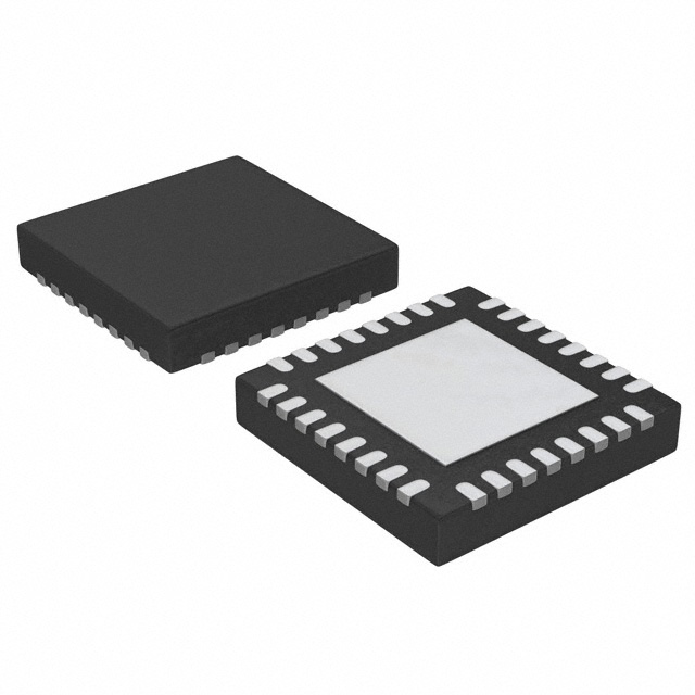
- Part No.:
- TDA18275HN/C1Y
- Manufacturer:
- NXP Semiconductors
- Category:
- Video Processing
- Package:
- 32-VFQFN Exposed Pad
- Datasheet:
-
 TDA18275HN/C1Y.pdf
- Description:
- IC VIDEO SILICON TUNER 32HVQFN
- Quantity:
- Payment:

- Shipping:

Inventory:4,364
Please send an inquiry. Send us your inquiry, and we will respond immediately.
Product details
Overview
TDA18275HN/C1Y from NXP Semiconductors is a hybrid silicon tuner IC for terrestrial and cable TV reception supporting both analog (NTSC, PAL, SECAM) and digital (DVB-T/T2, ATSC, ISDB-T) broadcast standards. It delivers Low IF (LIF) outputs at 1.7–10 MHz bandwidths with center frequencies from 0.8–7.5 MHz, integrates RF/IF selectivity and PLL-based LO synthesis, and operates from a single 3.3 V supply in HVQFN32 packaging.
For engineers reviewing the TDA18275HN/C1Y datasheet, TDA18275HN/C1Y pinout, TDA18275HN/C1Y application, or TDA18275HN/C1Y equivalent, key selection criteria include multistandard RF frequency coverage (42–1002 MHz), integrated Power Level Detector (PLD) and self-AGC synchronization for analog TV, dual IF output ports, and immunity to LTE/WLAN interferers - all critical for cost-sensitive, high-density TV and set-top box designs.
Technical Context
The TDA18275HN/C1Y implements a sigma-delta PLL architecture with LC-VCO and crystal oscillator, enabling precise local oscillator generation across its full 42–1002 MHz RF input range. Its fully integrated RF front-end includes a single-ended LNA, harmonic mixer, and on-chip RF tracking filters - eliminating external baluns and RF coils.
IF signal processing uses programmable complex filtering with two independent differential IF outputs (IFOUT_A_P/N and IFOUT_D_P/N), each supporting separate gain control (VIFAGC_A/D) and configurable channel bandwidths (1.7/6/7/8/10 MHz). The embedded PLD and temperature sensor provide real-time signal monitoring via I²C-bus interface compatible with 3.3 V microcontrollers.
Key Specifications
| Parameter | Value and Actual Design Meaning |
|---|---|
| RF Frequency Range | 42–1002 MHz - covers full VHF/UHF terrestrial and cable TV bands without external tuning elements. |
| Tuner Noise Figure | 3.3–4.5 dB - ensures high sensitivity for weak-signal reception in noisy urban environments. |
| Phase Jitter | 0.4–0.6° (250 Hz–4 MHz) - meets stringent timing stability requirements for digital demodulators. |
| Image Rejection | 65 dB - suppresses out-of-band interference without external image-reject filters. |
| IF Output Bandwidths | 1.7 / 6 / 7 / 8 / 10 MHz - matches legacy analog NTSC/PAL and modern DVB-T/T2/ATSC channel plans. |
| LIF Center Frequency Range | 0.8–7.5 MHz - enables flexible demodulator interface design across multiple SoC platforms. |
| Supply Voltage | 3.3 V ±10% - simplifies power delivery in consumer electronics with single-rail LDOs. |
| ESD Rating (HBM) | ±2 kV - meets IEC 61000-4-2 Level 3 for robust board-level handling and integration. |
Pinout & Package
HVQFN32 (SOT617-11), 5 × 5 × 0.85 mm, thermally enhanced, no leads, exposed thermal pad.
| Pin/Terminal | Circuit Role | Design Meaning |
|---|---|---|
| RFIN | Single-ended RF input | Accepts 75 Ω terrestrial/cable signal directly - no external balun required. |
| IFOUT_A_P / IFOUT_A_N | Differential analog IF output | Low-IF output for analog demodulators (e.g., NTSC/PAL); supports self-AGC via VSync. |
| IFOUT_D_P / IFOUT_D_N | Differential digital IF output | Configurable LIF output for DVB-T/T2/ATSC channel demodulators; independent gain control. |
| VIFAGC_A / VIFAGC_D | Analog/digital IF AGC voltage outputs | Provide analog control voltages to external IF amplifiers or internal gain stages. |
| GPO1 / GPO2 | Programmable general-purpose outputs | Configurable as logic-level signals for system control (e.g., filter switching, LNB power). |
| SCL / SDA | I²C-bus interface | 3.3 V-compatible serial control bus for configuration, status readback, and PLD monitoring. |
| XTAL_P / XTAL_N | Crysal oscillator inputs | Supports fundamental-mode quartz crystals (typically 16–27 MHz) for stable LO reference. |
| PLD | Power Level Detector output | Analog voltage proportional to RF input level - enables automatic signal strength indication. |
Key Features
| Feature | Design Value |
|---|---|
| Fully integrated RF selectivity | Eliminates need for external RF tracking filters and baluns - reduces BOM count by ≥12 passive components. |
| Dual independent IF paths | Enables simultaneous analog/digital TV reception or seamless standard migration without hardware change. |
| Embedded Power Level Detector (PLD) | Provides real-time RF signal strength monitoring via analog voltage - replaces external RSSI circuitry. |
| Self-AGC synchronization (VSync) | Automatically aligns IF gain control with vertical sync pulses in analog TV - eliminates manual alignment. |
| Strong LTE/WLAN immunity | Rejects interferers in digital dividend (698–806 MHz) and 2.4/5 GHz WLAN bands - improves reception in dense RF environments. |
| Programmable channel bandwidths | Five selectable IF bandwidths (1.7–10 MHz) allow one tuner design to support global analog and digital standards. |
Applications
| Smart TV Tuner Module | DVB-T2 Set-Top Box |
|---|---|
|
Use Scenario: Integrated terrestrial/cable tuner in 4K UHD smart TVs requiring dual-standard support and compact PCB layout. IC Role / Device Role / Timing Role: Primary RF-to-LIF converter with embedded PLL, AGC, and PLD - serves as front-end for main SoC demodulator. Use Value: Reduces tuner BOM by eliminating SAW filters, baluns, and discrete oscillators while maintaining <0.6° phase jitter for QAM256/OFDM demodulation. |
Use Scenario: Cost-optimized DVB-T2 receiver in emerging-market STBs needing high sensitivity and LTE coexistence. IC Role / Device Role / Timing Role: Multistandard silicon tuner delivering 8 MHz LIF output to DVB-T2 demodulator with integrated image rejection. Use Value: Achieves 65 dB image rejection and −70 dBc CTB performance without external filtering - enables single-layer RF section design. |
| Analog-to-Digital Transition Platform | Hybrid Broadcast Broadband TV (HbbTV) |
|
Use Scenario: Field-upgradable TV platforms supporting legacy NTSC/PAL and new DVB-T2 broadcasts in same hardware. IC Role / Device Role / Timing Role: Dual-path IF generator with independent analog/digital AGC and programmable bandwidth selection. Use Value: Enables software-selectable analog or digital mode using same PCB footprint - extends product lifecycle without redesign. |
Use Scenario: HbbTV-compliant receivers requiring simultaneous broadcast and IP stream processing with minimal latency. IC Role / Device Role / Timing Role: Low-jitter LIF source synchronized to video timing signals (VSync) for tight A/V alignment in hybrid decoding. Use Value: Self-AGC synchronization and <0.6° phase jitter ensure stable symbol timing recovery during broadcast/IP stream handover. |
Equivalent & Alternatives
The following parts are listed as comparable options for similar hybrid TV tuner applications.
| Alternative Part | Technical Difference | Application Difference | Selection Advice |
|---|---|---|---|
| MAX3543ETJ+T | Requires external crystal oscillator and balun; supports only DVB-T/T2 and ATSC - no analog TV capability. | Targeted at digital-only STBs; lacks VSync-driven AGC and PLD for analog signal monitoring. | Choose MAX3543ETJ+T when analog broadcast support is unnecessary and external component count is acceptable. |
| SI2151-A10-GM | Single IF output path; narrower RF range (42–870 MHz); no integrated PLD or VSync AGC mode. | Optimized for low-cost DVB-T2 receivers; not suitable for dual-standard or analog TV applications. | Choose SI2151-A10-GM for entry-level digital-only tuners where RF coverage above 870 MHz is not required. |
Compared with MAX3543ETJ+T and SI2151-A10-GM, the TDA18275HN/C1Y uniquely combines analog/digital multistandard operation, dual IF outputs, embedded PLD, and VSync AGC - making it the only option for true hybrid TV platforms requiring field-upgradeable analog-to-digital transition.
Availability
TDA18275HN/C1Y is available at Aetrix Electronics and suitable for smart TV tuner modules, DVB-T2 set-top boxes, hybrid broadcast broadband TV (HbbTV) receivers, and analog-to-digital transition platforms requiring stable component supply and long-term production continuity.
Supply support for TDA18275HN/C1Y includes scheduled delivery planning, volume procurement assistance, BOM continuity management, traceable sourcing, and lifecycle availability coordination for OEM customers, industrial embedded developers, connected-device designers, and electronics production programs.
Manufacturer
NXP Semiconductors is a global semiconductor company headquartered in Eindhoven, Netherlands, specializing in secure connectivity solutions for automotive, industrial, and consumer electronics.
The TDA18275HN/C1Y belongs to NXP's silicon TV tuner product line, designed specifically to replace legacy can-based tuners with fully integrated, multistandard RF front-ends for next-generation broadcast reception systems.
FAQ
What RF standards does the TDA18275HN/C1Y support?
The TDA18275HN/C1Y supports worldwide terrestrial and cable TV standards including analog NTSC, PAL, and SECAM, as well as digital DVB-T/T2, ATSC, and ISDB-T. Its 42–1002 MHz RF frequency range and programmable IF bandwidths (1.7–10 MHz) enable compliance with regional broadcast specifications without hardware modification. This multistandard capability is confirmed in the NXP TDA18275_SDS Rev. 2 datasheet.
Does the TDA18275HN/C1Y require external filters or baluns?
No, the TDA18275HN/C1Y integrates RF selectivity, harmonic filtering, and a single-ended LNA - eliminating the need for external baluns, RF tracking filters, or SAW devices. Its fully integrated architecture reduces tuner BOM count significantly, as stated in the "Features and benefits" section of the official short data sheet. This integration is validated by the block diagram showing on-chip LC-VCO, mixer, and IF filter stages.
How does the TDA18275HN/C1Y handle analog TV AGC synchronization?
The TDA18275HN/C1Y implements self-AGC synchronization (VSync mode) that automatically aligns IF gain control with vertical synchronization pulses in analog TV signals. This feature removes the need for manual alignment procedures during manufacturing or field service. The VSync functionality is explicitly documented in the "Features and benefits" list and supported by the dedicated VSync pin in the block diagram of the TDA18275_SDS Rev. 2.
What is the purpose of the two IF output ports on the TDA18275HN/C1Y?
The TDA18275HN/C1Y provides two independent differential IF output ports: IFOUT_A_P/N for analog demodulation and IFOUT_D_P/N for digital demodulation. Each path has dedicated gain control (VIFAGC_A/D) and supports configurable bandwidths. This dual-path architecture enables simultaneous analog/digital reception or seamless migration between broadcast standards using the same hardware platform - a key differentiator confirmed in the General Description section.
Is the TDA18275HN/C1Y suitable for environments with strong LTE or WLAN interference?
Yes, the TDA18275HN/C1Y features strong immunity to LTE interferers in the digital dividend band (698–806 MHz) and WLAN signals (802.11 a/b/g/n). This is achieved through on-chip image rejection (>65 dB) and optimized RF front-end filtering, as verified in the Quick Reference Data table and highlighted in the "Features and benefits" list. These characteristics make it suitable for urban deployments where co-location with cellular and Wi-Fi infrastructure is common.
TDA18275HN/C1Y Specifications
- Product attributes
- Attribute value
- Manufacturer:
- NXP Semiconductors
- Series:
- -
- Package/Case:
- 32-VFQFN Exposed Pad
- Packaging:
- Tape & Reel (TR)
- Product Status:
- Obsolete
- Function:
- Tuner
- Applications:
- Professional Video
- Standards:
- -
- Control Interface:
- I2C
- Voltage - Supply:
- 3.3V ~ 3.6V
- Mounting Type:
- Surface Mount
- Grade:
- -
- Qualification:
- -
- Supplier Device Package:
- 32-HVQFN (5x5)
TDA18275HN/C1Y FAQ
1.How can I place an order for TDA18275HN/C1Y through Aetrix?
Please submit a Request for Quotation (RFQ) for TDA18275HN/C1Y on Aetrix. Our sales agent will provide a competitive quotation and guide you through the order confirmation once you accept the terms.
2.Are the price and stock information for TDA18275HN/C1Y reliable?
The price and inventory of TDA18275HN/C1Y are updated periodically and may fluctuate due to market conditions. Stock and pricing data are typically refreshed every 24 hours. Quotation validity for TDA18275HN/C1Y is usually 5 days.
3.What payment methods are accepted for TDA18275HN/C1Y?
We accept Wire Transfer, PayPal, Credit Card, Western Union, MoneyGram, and Escrow for TDA18275HN/C1Y transactions.
Note: Certain payment methods may incur a processing fee.
4.How is shipping managed for TDA18275HN/C1Y?
TDA18275HN/C1Y orders can be shipped via leading logistics carriers, including DHL, UPS, FedEx, TNT, or Registered Mail.
Once your TDA18275HN/C1Y order is processed, you will receive an email with the shipment details and tracking number.
Note: Tracking information may take up to 24 hours to appear. Express delivery typically takes 3–5 business days.
5.How can I obtain technical support or documentation for TDA18275HN/C1Y?
For technical support, including TDA18275HN/C1Y datasheets, pinout diagrams, or application guidance, please contact our engineering support team. They can provide detailed documentation and assistance for your TDA18275HN/C1Y requirements.
6.How does Aetrix verify that TDA18275HN/C1Y is sourced from the original manufacturer or authorized distributors?
All TDA18275HN/C1Y products on Aetrix are procured from qualified distributors and authorized channels. Our dedicated quality assurance team conducts strict verification, including traceability checks and, if necessary, third-party testing. This ensures that TDA18275HN/C1Y meets industry standards.
7.What is the process for return or replacement of TDA18275HN/C1Y?
All TDA18275HN/C1Y units undergo pre-shipment inspection (PSI). If there is an issue with TDA18275HN/C1Y, returns or replacements are accepted under the following conditions:
1.Quantity discrepancies, incorrect items, or visible external defects (such as breakage or corrosion), acknowledged by Aetrix.
2.The issue is reported within 90 days of delivery.
3.The TDA18275HN/C1Y part is unused and in its original packaging.
Return procedure for TDA18275HN/C1Y:
1.Submit a request within 90 days.
2.Obtain a Return Material Authorization (RMA) from Aetrix.
TDA18275HN/C1Y Tags

-
HDMI2C1-6C1
STMicroelectronics

-
ADA4430-1YKSZ-R7
Analog Devices Inc.

-
LM1881MX/NOPB
Texas Instruments

-
SN75DP130SSRGZR
Texas Instruments

-
EQCO30T5.2
Microchip Technology

-
LMH1980MM/NOPB
Texas Instruments
-
EQCO30R5.D
Microchip Technology

-
SII9022ACNU
Lattice Semiconductor Corporation
-
SN65DP159RGZR
Texas Instruments

-
SN65DP159RSBR
Texas Instruments

-
SN65DP141RLJR
Texas Instruments

-
LMH0303SQ/NOPB
Texas Instruments
Tech Hub

A practical engineering guide to 3.3V and 5V logic compatibility, input thresholds, resistor dividers, translator ICs, MOSFET level shifting, I2C pull-ups, timing limits and power-sequencing risks.

The 74HC595 uses push-pull logic outputs, while the TPIC6B595 uses 50 V open-drain DMOS sinks for higher-power loads. This guide compares timing, current limits, 3.3 V interfacing, load wiring, thermal…

The 74HC595 converts serial data into eight stable parallel outputs. This guide covers pin functions, shift and storage timing, OE and MR behavior, drive-current limits, cascading, voltage compatibilit…

A technical comparison of level-sensitive latches and edge-triggered flip-flops, covering timing windows, setup and hold limits, master–slave operation, time borrowing, race-through, HDL inference and…

A D latch stores one bit while Enable controls when data can pass. This reference covers gate-level operation, truth tables, transparency, setup and hold timing, LE versus OE, common ICs and practical …

An SR latch stores one bit through cross-coupled feedback. This engineering reference covers NOR and NAND implementations, truth tables, forbidden-state recovery, gated operation, switch debouncing, fa…

Latch circuits retain one bit through feedback. This technical reference covers SR and D latches, truth tables, transparency, timing limits, latch-versus-flip-flop behavior, applications and common log…

An engineering guide to LED driver operation, constant-current and constant-voltage outputs, linear and switching topologies, dimming, IC selection, calculations, replacement compatibility, and fault c…

Operational amplifier guide covering op amp basics, feedback, ideal vs real op amps, common configurations, buffer circuits, offset, bias current, gain-bandwidth, slew rate, rail-to-rail limits and sel…

Jumper cables guide covering safe connection order, red and black clamp placement, final ground connection, cable gauge, length, clamp quality, copper vs CCA cables, jump starter comparison and battery…


