
 My Inquiry
 My Account


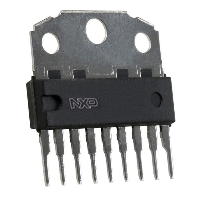
NXP Semiconductors TDA3602/N3,112
- Part No.:
- TDA3602/N3,112
- Manufacturer:
- NXP Semiconductors
- Package:
- 9-SIP Exposed Tab
- Datasheet:
-
 TDA3602/N3,112.pdf
- Description:
- IC REG LIN 8.5V/5V/5V 9-SIL MPF
- Quantity:
- Payment:

- Shipping:

Inventory:3,861
Please send an inquiry. Send us your inquiry, and we will respond immediately.
Product details
Overview
TDA3602/N3,112 from NXP Semiconductors (formerly Philips) is a triple-output automotive voltage regulator IC designed for car radio power management. It delivers fixed 8.5 V (REG1), 5.0 V (REG2), and 5.0 V (REG3) outputs with foldback current limiting, load dump protection up to 50 V, thermal shutdown, and microprocessor interface signals (RESET/HOLD). It operates across −6 V to 50 V supply range and supports coma-mode quiescent current of 290 µA - critical for battery-backed infotainment systems.
For engineers reviewing the TDA3602/N3,112 datasheet, TDA3602/N3,112 pinout, TDA3602/N3,112 application, or TDA3602/N3,112 equivalent, this page provides verified technical context, validated pin functions, confirmed regulator specifications under load-dump and thermal-shutdown conditions, and real-world automotive use cases including microprocessor reset sequencing, mute control, and backup power holdover during engine cranking.
Technical Context
The TDA3602/N3,112 integrates three independent linear regulators with distinct operational states controlled by an internal Schmitt-trigger-based state machine driven by the Vsc (pin 4) input. REG1 and REG2 are VP-controlled and switchable between ON/OFF via Vsc thresholds (e.g., wake at 2.8 V, sleep at 3.6 V, coma at >3.8 V), while REG3 remains active during load dump and thermal shutdown, powered via internal back-up switch and external capacitor on Vbu (pin 8).
Its protection architecture includes foldback current limiting on REG1/REG2 (0.4–1.2 A), reverse-polarity safety on VP (pin 1), DC short-circuit tolerance to ground and VP, and Zener-clamped Vbu capable of withstanding 50 V load dump pulses when supplied through a 100 Ω series resistor. RESET (pin 3) asserts LOW during load dump; HOLD (pin 5) toggles based on VP and regulator regulation status per Table 2.
Key Specifications
| Parameter | Value and Actual Design Meaning |
|---|---|
| Supply voltage range | −6 V to 50 V - withstands reverse battery, jump-start (30 V/10 min), and load dump (50 V/50 ms) without external protection |
| REG1 output voltage | 8.5 V ±0.3 V (8.2–8.8 V) at 0.5–250 mA - powers audio preamp stages and analog circuitry in car radios |
| REG2 & REG3 output voltage | 5.0 V ±0.2 V (4.8–5.2 V) each at up to 140 mA (REG2) and 50 mA (REG3) - supplies digital logic and microcontroller core/peripherals |
| Quiescent current (coma mode) | 290 µA typical at VP = 14.4 V - enables <10 µA system standby current when paired with microcontroller sleep modes |
| RESET output behavior | Active-LOW during load dump or VP < 7.3 V - provides hardware reset signal to 80C51-class MCUs without external supervision IC |
| Vbu (pin 8) back-up capability | Supports electrolytic capacitor hold-up for REG3 during negative field decay or engine start - sustains microcontroller operation for ~100–500 ms post-supply loss |
| Thermal protection | Triggers at Tvj = 150 °C - disables REG1/REG2 while maintaining REG3 output to preserve MCU watchdog/reset functionality |
Pinout & Package
Package: SOT110-1 (9-pin plastic SIP), lead pitch 2.54 mm, body width 7.62 mm, height 4.2 mm - designed for through-hole mounting in automotive PCBs with high mechanical robustness.
| Pin/Terminal | Circuit Role | Design Meaning |
|---|---|---|
| VP (pin 1) | Positive supply input | Accepts −6 V to 50 V; reverse-polarity safe; feeds all regulators and internal protection circuits |
| REG1 (pin 2) | 8.5 V regulator output | Fixed 8.5 V output with foldback current limit (0.4–1.2 A); disabled in sleep/coma modes |
| RESET (pin 3) | Reset output signal | Open-collector, active-LOW during load dump, VP undervoltage (<7.3 V), or power-on initialization |
| Vsc (pin 4) | State control input | Four-state Schmitt-trigger input (thresholds: 1.1 V, 2.2 V, 2.8 V, 3.6 V, 3.8 V) controlling ON/SLEEP/COMA/WAKE modes |
| HOLD (pin 5) | Hold output signal | Open-collector, HIGH only when REG1/REG2 are regulated AND VP Schmitt trigger is true - used for mute control or MCU interrupt |
| GND (pin 6) | Ground reference | Common return for all regulators and logic; must be low-impedance connection to chassis ground in automotive layout |
| REG3 (pin 7) | 5.0 V backup regulator output | Always-active 5 V output; continues supplying MCU during load dump, thermal shutdown, or VP interruption |
| Vbu (pin 8) | Back-up capacitor terminal | Connects to electrolytic capacitor; internal switch isolates it during normal operation and engages it during VP drop or load dump |
| REG2 (pin 9) | 5.0 V regulator output | Fixed 5.0 V output with foldback current limit (200–600 mA); disabled in sleep/coma modes |
Key Features
| Feature | Design Value |
|---|---|
| Triple independent regulator outputs | 8.5 V (REG1), 5.0 V (REG2), and 5.0 V (REG3) - enables single-chip power for analog, digital, and MCU domains in car radios |
| Load dump survival | Withstands 50 V transients on VP and Vbu (with 100 Ω series resistor) - eliminates need for external TVS diodes in basic designs |
| Microprocessor interface signals | Integrated RESET (power-on/load dump) and HOLD (regulation status) outputs - reduces BOM count vs discrete supervisor + GPIO solutions |
| Low-power coma mode | 290 µA total quiescent current - allows full system standby with MCU in deep sleep, meeting automotive ISO 8859-3 leakage requirements |
| Vbu back-up circuit | Internal switch + external capacitor sustains REG3 output for short-term VP loss - supports MCU firmware recovery after engine cranking |
| Foldback current limiting | Reduces power dissipation during short-circuit faults on REG1/REG2 - prevents thermal runaway and improves reliability in unregulated 12 V environments |
Applications
| Car Radio Power Management | Microprocessor Reset Sequencing |
|---|---|
Use Scenario: Powering analog audio stages, digital logic, and 80C51-class MCU in OEM car stereo head units with ignition-switched and battery-backed operation. IC Role / Device Role / Timing Role: Central voltage regulator providing three isolated rails, managing state transitions (ON/SLEEP/COMA), and generating hardware reset on supply fault. Use Value: Eliminates need for separate LDOs, reset supervisors, and back-up switches - reduces board space by ≥30% and component count by ≥5 parts. |
Use Scenario: Ensuring deterministic MCU boot after power-on, key-press wake-up, or load dump recovery in infotainment systems. IC Role / Device Role / Timing Role: Generates synchronized RESET pulse (HIGH at power-on, LOW at load dump) and HOLD signal indicating regulator health for MCU firmware decision-making. Use Value: Enables zero-software-reset latency and guaranteed power-on initialization - avoids corrupted EEPROM writes or missed security code entry windows. |
| Mute Control for Audio Amplifiers | Engine Cranking Holdover Support |
Use Scenario: Controlling amplifier mute inputs during power-up, fault conditions, or sleep transitions in low-end car radios without microcontrollers. IC Role / Device Role / Timing Role: HOLD output drives mute transistor directly; asserts HIGH only when both REG1 and REG2 are in regulation and VP is stable. Use Value: Prevents speaker pop/noise during turn-on/turn-off and automatically mutes during VP sag - no external logic or timing components required. |
Use Scenario: Maintaining MCU operation during engine start when battery voltage drops below 6 V for up to 500 ms. IC Role / Device Role / Timing Role: Vbu pin charges external capacitor during normal operation; internal switch connects it to REG3 during VP collapse to sustain 5 V output. Use Value: Guarantees uninterrupted MCU watchdog timer and RAM retention - avoids system hang or security lockout during cold starts. |
Equivalent & Alternatives
The following parts are listed as comparable options for similar multiple-output automotive voltage regulator applications.
| Alternative Part | Technical Difference | Application Difference | Selection Advice |
|---|---|---|---|
| TLF4941-2ES | Single 5 V output (no 8.5 V rail); integrated watchdog and window comparator; QFN-32 package | Requires external 8.5 V LDO for analog stages; better suited for modern CAN-based ECUs than legacy car radios | Select if migrating to ASIL-B compliant design with diagnostic features; not drop-in for TDA3602/N3,112 footprint or 8.5 V requirement |
| MAX16920ATP+ | Dual output (5 V/3.3 V); higher quiescent current (35 µA min); supports 65 V load dump; TQFN-20 | Lacks dedicated back-up capacitor pin and coma-mode ultra-low IQ; targets ADAS cameras, not infotainment | Choose for 3.3 V logic compatibility and extended load dump margin; requires redesign of Vbu holdover and state control interface |
Compared with TLF4941-2ES and MAX16920ATP+, the TDA3602/N3,112 uniquely delivers an 8.5 V analog rail, sub-300 µA coma current, and pin-specific Vbu holdover - making it irreplaceable in cost-sensitive, legacy car radio platforms requiring minimal external components and proven field reliability.
Availability
TDA3602/N3,112 is available at Aetrix Electronics and suitable for automotive infotainment, car radio power management, and microprocessor-based embedded systems requiring stable component supply across extended temperature ranges and harsh electrical environments.
Supply support for TDA3602/N3,112 includes scheduled delivery planning, volume procurement assistance, BOM continuity management, traceable sourcing, and lifecycle availability coordination for OEM customers, industrial embedded developers, connected-device designers, and electronics production programs.
Manufacturer
NXP Semiconductors is a global semiconductor leader focused on secure connectivity solutions for automotive, industrial, and IoT applications, with heritage in Philips' analog power IC portfolio.
The TDA3602/N3,112 belongs to NXP's legacy automotive power management family, specifically engineered for cost-effective, robust power delivery in car radios - balancing integration, protection, and ultra-low standby power without MCU dependency.
FAQ
What is the maximum load dump voltage the TDA3602/N3,112 can withstand on the VP pin?
The TDA3602/N3,112 withstands load dump pulses up to 50 V on the VP pin for durations ≤50 ms with rise time ≥2.5 ms, as specified in the Absolute Maximum Ratings table. This rating applies with no external protection required, provided the device is operated within its thermal limits and the Vbu pin is appropriately configured with a 100 Ω series resistor if sourced from VP2.
How does the TDA3602/N3,112 maintain microprocessor operation during engine cranking?
The TDA3602/N3,112 maintains microprocessor operation during engine cranking via its Vbu (pin 8) back-up circuit: an external electrolytic capacitor charges during normal operation, and an internal switch connects it to REG3 (pin 7) when VP drops below ~7.3 V. This sustains the 5.0 V output for ~100–500 ms, allowing the MCU to complete critical tasks before entering safe shutdown.
What are the exact voltage thresholds on the Vsc (state control) pin for mode transitions?
The TDA3602/N3,112 uses hysteresis-equipped Schmitt triggers on Vsc (pin 4): ON-to-RESET transition occurs at 2.0 V (falling), RESET-to-WAKE at 2.8 V (rising), WAKE-to-SLEEP at 3.6 V (rising), and SLEEP-to-COMA at >3.8 V (rising). Falling thresholds are ~0.9 V lower due to 0.92 V hysteresis, ensuring noise-immune state switching in automotive EMI environments.
Can the TDA3602/N3,112 be used without a microprocessor?
Yes, the TDA3602/N3,112 supports microprocessor-less operation: Fig.7 and Fig.8 in the datasheet show low-end car radio implementations using push-button switches and discrete transistors to drive the Vsc pin and interpret HOLD output for mute control. In such configurations, RESET and HOLD serve as direct logic-level signals for power amplifiers and status indication without MCU intervention.
What is the purpose of the HOLD output, and how is it generated?
The HOLD output (pin 5) is an open-collector signal that goes HIGH only when both REG1 and REG2 are in regulation AND the VP Schmitt trigger is satisfied (VP > 7.6 V). It reflects real-time regulator health and supply stability - used directly to enable audio power stages or generate MCU interrupts. Its logic is defined in Table 2 and is independent of Vsc state, making it a reliable fault indicator.
TDA3602/N3,112 Specifications
- Product attributes
- Attribute value
- Manufacturer:
- NXP Semiconductors
- Series:
- -
- Package/Case:
- 9-SIP Exposed Tab
- Packaging:
- Tube
- Product Status:
- Obsolete
- Output Configuration:
- Positive
- Output Type:
- Fixed
- Number of Regulators:
- 3
- Voltage - Input (Max):
- 18V
- Voltage - Output (Min/Fixed):
- 8.5V, 5V, 5V
- Voltage - Output (Max):
- -
- Voltage Dropout (Max):
- 0.4V @ 250mA, 1.2V @ 140mA (Typ), 0.4V @ 50mA
- Current - Output:
- 250mA, 140mA, 50mA
- Current - Quiescent (Iq):
- 360 µA
- Current - Supply (Max):
- -
- PSRR:
- 60dB (200Hz)
- Control Features:
- Reset
- Protection Features:
- Load Dump, Over Current, Over Temperature, Reverse Polarity, Short Circuit
- Operating Temperature:
- -40°C ~ 150°C
- Grade:
- -
- Qualification:
- -
- Mounting Type:
- Through Hole
- Supplier Device Package:
- 9-SIL MPF
TDA3602/N3,112 FAQ
1.How can I place an order for TDA3602/N3,112 through Aetrix?
Please submit a Request for Quotation (RFQ) for TDA3602/N3,112 on Aetrix. Our sales agent will provide a competitive quotation and guide you through the order confirmation once you accept the terms.
2.Are the price and stock information for TDA3602/N3,112 reliable?
The price and inventory of TDA3602/N3,112 are updated periodically and may fluctuate due to market conditions. Stock and pricing data are typically refreshed every 24 hours. Quotation validity for TDA3602/N3,112 is usually 5 days.
3.What payment methods are accepted for TDA3602/N3,112?
We accept Wire Transfer, PayPal, Credit Card, Western Union, MoneyGram, and Escrow for TDA3602/N3,112 transactions.
Note: Certain payment methods may incur a processing fee.
4.How is shipping managed for TDA3602/N3,112?
TDA3602/N3,112 orders can be shipped via leading logistics carriers, including DHL, UPS, FedEx, TNT, or Registered Mail.
Once your TDA3602/N3,112 order is processed, you will receive an email with the shipment details and tracking number.
Note: Tracking information may take up to 24 hours to appear. Express delivery typically takes 3–5 business days.
5.How can I obtain technical support or documentation for TDA3602/N3,112?
For technical support, including TDA3602/N3,112 datasheets, pinout diagrams, or application guidance, please contact our engineering support team. They can provide detailed documentation and assistance for your TDA3602/N3,112 requirements.
6.How does Aetrix verify that TDA3602/N3,112 is sourced from the original manufacturer or authorized distributors?
All TDA3602/N3,112 products on Aetrix are procured from qualified distributors and authorized channels. Our dedicated quality assurance team conducts strict verification, including traceability checks and, if necessary, third-party testing. This ensures that TDA3602/N3,112 meets industry standards.
7.What is the process for return or replacement of TDA3602/N3,112?
All TDA3602/N3,112 units undergo pre-shipment inspection (PSI). If there is an issue with TDA3602/N3,112, returns or replacements are accepted under the following conditions:
1.Quantity discrepancies, incorrect items, or visible external defects (such as breakage or corrosion), acknowledged by Aetrix.
2.The issue is reported within 90 days of delivery.
3.The TDA3602/N3,112 part is unused and in its original packaging.
Return procedure for TDA3602/N3,112:
1.Submit a request within 90 days.
2.Obtain a Return Material Authorization (RMA) from Aetrix.
TDA3602/N3,112 Tags

-
MIC5504-1.8YM5-TR
Microchip Technology
-
MIC5504-3.3YM5-TR
Microchip Technology

-
MIC5365-3.0YC5-TR
Microchip Technology
-
MIC5365-1.8YC5-TR
Microchip Technology
-
MIC5365-2.5YC5-TR
Microchip Technology
-
MIC5365-3.3YC5-TR
Microchip Technology

-
MIC5365-3.3YD5-TR
Microchip Technology

-
MIC5317-3.3YM5-TR
Microchip Technology

-
TLV1117LV33DCYR
Texas Instruments

-
MIC5317-3.3YMT-TZ
Microchip Technology

-
MIC5528-3.3YMT-TR
Microchip Technology

-
TLV75801PDRVR
Texas Instruments
Tech Hub

An SR latch stores one bit through cross-coupled feedback. This engineering reference covers NOR and NAND implementations, truth tables, forbidden-state recovery, gated operation, switch debouncing, fa…

Latch circuits retain one bit through feedback. This technical reference covers SR and D latches, truth tables, transparency, timing limits, latch-versus-flip-flop behavior, applications and common log…

An engineering guide to LED driver operation, constant-current and constant-voltage outputs, linear and switching topologies, dimming, IC selection, calculations, replacement compatibility, and fault c…

Operational amplifier guide covering op amp basics, feedback, ideal vs real op amps, common configurations, buffer circuits, offset, bias current, gain-bandwidth, slew rate, rail-to-rail limits and sel…

Jumper cables guide covering safe connection order, red and black clamp placement, final ground connection, cable gauge, length, clamp quality, copper vs CCA cables, jump starter comparison and battery…

LDO regulator guide covering low dropout voltage, power dissipation, thermal design, PSRR, output noise, capacitor stability, adjustable LDO circuits, LDO vs buck converter and datasheet selection chec…

Conditional Access Module guide covering CAM meaning, CI/CI+ interface, smart card authorization, DVB security workflow, TV and set-top box compatibility, internal electronics, ESD protection, connecto…

Guide to electronic component obsolescence covering EOL risk, PCN/PDN notices, last-time buy planning, replacement options, form-fit-function validation, counterfeit risk and BOM lifecycle management.

18650 battery guide covering lithium-ion cell basics, 3.6V/3.7V voltage, 4.2V charging, mAh and Wh capacity, protected cells, chargers, BMS, series-parallel packs, holders, welding and sourcing checks.…

Hall effect sensor guide covering working principle, linear and digital sensors, Arduino circuits, current sensing, speed detection, automotive applications, A3144 examples, signal filtering and datash…


