
 My Inquiry
 My Account


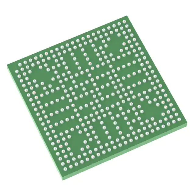
Texas Instruments TDA3MVRBFABFRQ1
- Part No.:
- TDA3MVRBFABFRQ1
- Manufacturer:
- Texas Instruments
- Category:
- System On Chip (SoC)
- Package:
- 367-BFBGA, FCBGA
- Datasheet:
-
 TDA3MVRBFABFRQ1.pdf
- Description:
- IC SOC PROCESSOR
- Quantity:
- Payment:

- Shipping:

Inventory:4,803
Please send an inquiry. Send us your inquiry, and we will respond immediately.
Product details
Overview
TDA3MVRBFABFRQ1 from Texas Instruments is an automotive-qualified System-on-Chip (SoC) designed for Advanced Driver Assistance Systems (ADAS), integrating dual C66x DSPs, dual Arm® Cortex®-M4 IPU cores, Embedded Vision Engine (EVE), 512kB on-chip L3 RAM, and support for DDR3/DDR3L up to 1066 MT/s - deployed in front camera, surround-view, and sensor fusion systems.
For engineers reviewing the TDA3MVRBFABFRQ1 datasheet, TDA3MVRBFABFRQ1 pinout, TDA3MVRBFABFRQ1 application, or TDA3MVRBFABFRQ1 equivalent, this page delivers verified technical context, validated package mapping, confirmed ADAS-specific peripherals (MIPI CSI-2, DCAN/MCAN, GMAC), and real-world functional alternatives aligned to AEC-Q100 Grade 2 requirements.
Technical Context
The TDA3MVRBFABFRQ1 implements a heterogeneous processing architecture with two independent C66x VLIW DSPs (floating-point capable, object-code compatible with C64x+/C67x), dual Cortex-M4 Image Processing Units (IPUs) with ECC, and a dedicated EVE coprocessor optimized for vision analytics offload - enabling parallel execution of ISP pipelines, WDR/LDC correction, and real-time object detection.
It integrates a full hardware image pipe (DPC, CFA, 3D-NF, RGB-YUV), MIPI CSI-2 v1.0 receiver supporting up to 4-lane input, dual 3-port Gigabit Ethernet switch (RGMII only), dual CAN interfaces (DCAN + MCAN with CAN 2.0B), and safety-critical subsystems including TESOC (LBIST/PBIST), Error Signaling Module (ESM), and five Real-Time Interrupt (RTI) modules usable as watchdog timers.
Key Specifications
| Parameter | Value and Actual Design Meaning |
|---|---|
| Core Architecture | Dual TMS320C66x DSP + dual Arm Cortex-M4 IPU + EVE vision coprocessor - enables concurrent high-throughput vision analytics and real-time control. |
| Memory Interface | EMIF supports DDR3/DDR3L up to 1066 MT/s, DDR2 up to 800 MT/s, LPDDR2 up to 667 MT/s - provides ≥2GB addressable memory space for multi-camera buffer storage. |
| Video Input | MIPI CSI-2 v1.0 (5-lane max), VIP supporting up to 4 multiplexed ports - enables simultaneous connection of multiple cameras (e.g., front + side + rear). |
| ADC | 8-channel 10-bit SAR ADC - used for on-die temperature monitoring and external analog sensor interfacing (e.g., voltage/current sensing). |
| Safety Compliance | AEC-Q100 Grade 2 qualified (−40°C to +105°C), integrated ESM, CRC, DCC, RTI, and TESOC LBIST/PBIST - meets ASIL-B system-level requirements. |
| Package | 367-ball FCBGA (ABF), 15 mm × 15 mm, 0.65 mm pitch - supports automotive thermal and mechanical reliability standards. |
| Peripherals | 3× McASP, 4× McSPI, QSPI, 2× I²C, 3× UART, SDIO, GPMC, PWMSS, 126 GPIO - enables flexible connectivity to radar, ultrasonic, display, and actuator subsystems. |
Pinout & Package
367-ball FCBGA (ABF) package, 15.0 mm × 15.0 mm body size, 0.65 mm ball pitch. Ball grid includes dedicated power/ground arrays, DDR interface banks (ddr1_a0–ddr1_dqsn_ecc), MIPI CSI-2 lanes (csi2_0_dx0–csi2_0_dy4), CAN transceivers (dcan1_rx/tx), and ADC inputs (adc_in0–adc_in7).
| Pin/Terminal | Circuit Role | Design Meaning |
|---|---|---|
| adc_in0–adc_in7 | Analog input channels | Connect to on-die temperature sensor or external analog sensors; referenced to adc_vrefp for 10-bit conversion accuracy. |
| csi2_0_dx0–csi2_0_dy4 | MIPI CSI-2 differential data/lane clock | Receive serialized image data from up to 5-lane camera sensors; require controlled impedance routing and AC coupling. |
| ddr1_ck / ddr1_nck | DDR clock and inverted clock | Drive DDR3/DDR3L memory timing; must be length-matched and routed differentially with tight skew control. |
| dcan1_rx / dcan1_tx | Controller Area Network interface | Support CAN 2.0B protocol at up to 1 Mbps; require external CAN transceiver and termination resistors. |
| vdda_adc / vdda_csi / vdds_ddr1 | Power supply domains | Independent voltage rails for analog ADC, MIPI CSI-2, and DDR I/O - mandate separate low-noise LDO regulation and decoupling. |
Key Features
| Feature | Design Value |
|---|---|
| Vision AccelerationPac (EVE) | 32-bit RISC core + vector coprocessor dedicated to vision analytics - reduces CPU load by offloading stereo matching, optical flow, and feature extraction. |
| Full HW Image Pipe | Integrated DPC, CFA, 3D-NF, RGB-YUV conversion, WDR, and lens distortion correction (LDC) - eliminates need for external ISP FPGA or ASIC. |
| Display Subsystem | Display controller with DMA engine + CVIDEO/SD-DAC analog composite output - enables direct connection to rearview mirrors or cabin displays without external DAC. |
| Safety-Critical Subsystems | TESOC (LBIST/PBIST), ESM, CRC, 7× Dual Clock Comparators (DCC), 5× RTI - enables ISO 26262-compliant diagnostic coverage for ASIL-B applications. |
| Automotive Connectivity | 3-port Gigabit Ethernet switch (RGMII), dual CAN (DCAN + MCAN), MIPI CSI-2, LVDS-RX - supports sensor fusion architectures combining camera, radar, and ultrasonic data. |
Applications
| Front Camera ADAS | Surround-View System |
|---|---|
|
Use Scenario: Mono/stereo front-facing camera capturing traffic signs, lane markings, pedestrians, and vehicles at 60 fps Full HD resolution. IC Role / Device Role / Timing Role: Primary vision SoC performing real-time ISP pipeline, object detection, and decision logic using dual C66x DSPs and EVE. Use Value: Enables automatic emergency braking and adaptive cruise control with <100 ms end-to-end latency via hardware-accelerated image processing. |
Use Scenario: 4-camera LVDS-based surround-view system generating stitched 2D/3D top-down view for parking assist and drive recording. IC Role / Device Role / Timing Role: Central processor aggregating video streams via VIP and MIPI CSI-2, executing mesh warping and blending in EVE and DSP subsystems. Use Value: Delivers seamless 360° visualization with sub-pixel geometric correction using on-chip LDC and perspective transform engines. |
| Sensor Fusion Hub | Rear Camera Monitoring |
|
Use Scenario: Integration point for camera, radar, and ultrasonic sensor data to perform raw or object-level fusion for collision avoidance. IC Role / Device Role / Timing Role: High-bandwidth interconnect hub using GMAC switch and EDMA to synchronize time-stamped sensor inputs across heterogeneous interfaces. Use Value: Achieves synchronized multi-sensor timestamping within ±1 µs using hardware timer synchronization and GMAC PTP support. |
Use Scenario: Rear-facing camera providing backup assistance with dynamic guidelines, pedestrian detection, and obstacle classification. IC Role / Device Role / Timing Role: Dedicated imaging subsystem (ISS) with MIPI CSI-2 input, hardware ISP pipeline, and SD-DAC analog output to rearview display. Use Value: Supports WDR and low-light enhancement for nighttime operation while maintaining <50 ms display-to-actuation latency. |
Equivalent & Alternatives
The following parts are listed as comparable options for similar ADAS vision processing applications.
| Alternative Part | Technical Difference | Application Difference | Selection Advice |
|---|---|---|---|
| TDA3MAABFABFRQ1 | Single C66x DSP core (vs. dual in TDA3MVRBFABFRQ1); no Display Subsystem (VOUT1/SD_DAC); 256kB OCMC RAM (vs. 512kB) | Targeted at cost-sensitive mono-camera ADAS; lacks analog video output and second DSP for parallel analytics | Select when full dual-DSP performance and display output are unnecessary; lower BOM cost but reduced vision throughput |
| TDA3MDABFABFRQ1 | Single C66x DSP; no EVE; no ISS (MIPI CSI-2 disabled); no WDR/LDC hardware blocks | Designed for non-vision roles (e.g., radar pre-processing, gateway functions); no camera interface capability | Choose only for non-imaging ADAS subsystems requiring DSP compute without vision acceleration or camera I/O |
Compared with TDA3MAABFABFRQ1 and TDA3MDABFABFRQ1, the TDA3MVRBFABFRQ1 uniquely delivers dual-DSP concurrency, full hardware image pipe (WDR/LDC), MIPI CSI-2, and analog video output - making it the only variant suitable for production front/surround-view ADAS systems requiring ASIL-B compliance and real-time vision analytics.
Availability
TDA3MVRBFABFRQ1 is available at Aetrix Electronics and suitable for automotive front camera, surround-view, and sensor fusion applications requiring stable component supply, long-term lifecycle support, and AEC-Q100-compliant sourcing.
Supply support for TDA3MVRBFABFRQ1 includes scheduled delivery planning, volume procurement assistance, BOM continuity management, traceable sourcing, and lifecycle availability coordination for OEM customers, industrial embedded developers, connected-device designers, and electronics production programs.
Manufacturer
Texas Instruments is a global semiconductor company specializing in analog, embedded processing, and automotive ICs, with leadership in ADAS, power management, and signal chain technologies.
The TDA3x product line was engineered specifically for scalable, low-power automotive vision processing - balancing computational density, thermal efficiency, and functional safety to enable next-generation autonomous driving features.
FAQ
What is the silicon revision and package type of TDA3MVRBFABFRQ1?
TDA3MVRBFABFRQ1 uses Silicon Revision 2.0 and is packaged in a 367-ball FCBGA (ABF) with 15 mm × 15 mm body size and 0.65 mm pitch. This package is qualified for automotive use per AEC-Q100 Grade 2 and supports thermal dissipation requirements for sustained ADAS workloads.
Does TDA3MVRBFABFRQ1 support CAN FD or only classical CAN 2.0B?
TDA3MVRBFABFRQ1 integrates both DCAN and MCAN modules compliant with CAN 2.0B protocol. While MCAN supports optional CAN FD functionality, the TDA3MVRBFABFRQ1 datasheet confirms CAN FD is not enabled in this specific variant - only classical CAN 2.0B at up to 1 Mbps is supported.
What memory types and speeds does the EMIF in TDA3MVRBFABFRQ1 support?
The EMIF in TDA3MVRBFABFRQ1 supports DDR3/DDR3L up to 1066 MT/s, DDR2 up to 800 MT/s, and LPDDR2 up to 667 MT/s, with up to 2GB total addressable memory space. It includes optional SECDED ECC for DDR interfaces to meet ASIL-B data integrity requirements.
Is the Embedded Vision Engine (EVE) present and functional in TDA3MVRBFABFRQ1?
Yes, TDA3MVRBFABFRQ1 includes one fully functional EVE1 coprocessor - a dedicated 32-bit RISC core with vector coprocessor optimized for vision analytics offload. It accelerates tasks including stereo matching, optical flow, and feature extraction independently of the main DSPs and CPUs.
What is the maximum video resolution and frame rate supported by TDA3MVRBFABFRQ1's video input subsystem?
TDA3MVRBFABFRQ1 supports Full-HD video input at 1920 × 1080p resolution and 60 fps via its Video Input Port (VIP) and MIPI CSI-2 interface. The hardware image pipe (DPC, CFA, 3D-NF) processes this stream in real time with WDR and lens distortion correction enabled.
TDA3MVRBFABFRQ1 Specifications
- Product attributes
- Attribute value
- Manufacturer:
- Texas Instruments
- Series:
- -
- Package/Case:
- 367-BFBGA, FCBGA
- Packaging:
- Tape & Reel (TR)
- Product Status:
- Active
- Architecture:
- DSP, MPU
- Core Processor:
- ARM® Cortex®-M4, C66x
- Flash Size:
- -
- RAM Size:
- 512kB
- Peripherals:
- DMA, PWM, WDT
- Connectivity:
- CAN, MMC/SD/SDIO, McASP, I2C, SPI, UART, USB
- Speed:
- 212.8MHz, 745MHz
- Primary Attributes:
- -
- Operating Temperature:
- -40°C ~ 125°C (TJ)
- Grade:
- -
- Qualification:
- -
- Supplier Device Package:
- 367-FCBGA (15x15)
TDA3MVRBFABFRQ1 FAQ
1.How can I place an order for TDA3MVRBFABFRQ1 through Aetrix?
Please submit a Request for Quotation (RFQ) for TDA3MVRBFABFRQ1 on Aetrix. Our sales agent will provide a competitive quotation and guide you through the order confirmation once you accept the terms.
2.Are the price and stock information for TDA3MVRBFABFRQ1 reliable?
The price and inventory of TDA3MVRBFABFRQ1 are updated periodically and may fluctuate due to market conditions. Stock and pricing data are typically refreshed every 24 hours. Quotation validity for TDA3MVRBFABFRQ1 is usually 5 days.
3.What payment methods are accepted for TDA3MVRBFABFRQ1?
We accept Wire Transfer, PayPal, Credit Card, Western Union, MoneyGram, and Escrow for TDA3MVRBFABFRQ1 transactions.
Note: Certain payment methods may incur a processing fee.
4.How is shipping managed for TDA3MVRBFABFRQ1?
TDA3MVRBFABFRQ1 orders can be shipped via leading logistics carriers, including DHL, UPS, FedEx, TNT, or Registered Mail.
Once your TDA3MVRBFABFRQ1 order is processed, you will receive an email with the shipment details and tracking number.
Note: Tracking information may take up to 24 hours to appear. Express delivery typically takes 3–5 business days.
5.How can I obtain technical support or documentation for TDA3MVRBFABFRQ1?
For technical support, including TDA3MVRBFABFRQ1 datasheets, pinout diagrams, or application guidance, please contact our engineering support team. They can provide detailed documentation and assistance for your TDA3MVRBFABFRQ1 requirements.
6.How does Aetrix verify that TDA3MVRBFABFRQ1 is sourced from the original manufacturer or authorized distributors?
All TDA3MVRBFABFRQ1 products on Aetrix are procured from qualified distributors and authorized channels. Our dedicated quality assurance team conducts strict verification, including traceability checks and, if necessary, third-party testing. This ensures that TDA3MVRBFABFRQ1 meets industry standards.
7.What is the process for return or replacement of TDA3MVRBFABFRQ1?
All TDA3MVRBFABFRQ1 units undergo pre-shipment inspection (PSI). If there is an issue with TDA3MVRBFABFRQ1, returns or replacements are accepted under the following conditions:
1.Quantity discrepancies, incorrect items, or visible external defects (such as breakage or corrosion), acknowledged by Aetrix.
2.The issue is reported within 90 days of delivery.
3.The TDA3MVRBFABFRQ1 part is unused and in its original packaging.
Return procedure for TDA3MVRBFABFRQ1:
1.Submit a request within 90 days.
2.Obtain a Return Material Authorization (RMA) from Aetrix.
TDA3MVRBFABFRQ1 Tags

-
AMA3B1KK-KCR-TB
Ambiq Micro, Inc.

-
AMA4B2KP-KBR
Ambiq Micro, Inc.
-
SC-20100S-A
GHI Electronics, LLC
-
M2S010-TQG144I
Microchip Technology
-
A2F200M3F-FGG256I
Microchip Technology
-
M2S010TS-1VFG256I
Microchip Technology
-
XC7Z010-1CLG225C
AMD
-
M2S025-FCSG325I
Microchip Technology
-
XC7Z010-1CLG400C
AMD
Tech Hub

A practical engineering guide to 3.3V and 5V logic compatibility, input thresholds, resistor dividers, translator ICs, MOSFET level shifting, I2C pull-ups, timing limits and power-sequencing risks.

The 74HC595 uses push-pull logic outputs, while the TPIC6B595 uses 50 V open-drain DMOS sinks for higher-power loads. This guide compares timing, current limits, 3.3 V interfacing, load wiring, thermal…

The 74HC595 converts serial data into eight stable parallel outputs. This guide covers pin functions, shift and storage timing, OE and MR behavior, drive-current limits, cascading, voltage compatibilit…

A technical comparison of level-sensitive latches and edge-triggered flip-flops, covering timing windows, setup and hold limits, master–slave operation, time borrowing, race-through, HDL inference and…

A D latch stores one bit while Enable controls when data can pass. This reference covers gate-level operation, truth tables, transparency, setup and hold timing, LE versus OE, common ICs and practical …

An SR latch stores one bit through cross-coupled feedback. This engineering reference covers NOR and NAND implementations, truth tables, forbidden-state recovery, gated operation, switch debouncing, fa…

Latch circuits retain one bit through feedback. This technical reference covers SR and D latches, truth tables, transparency, timing limits, latch-versus-flip-flop behavior, applications and common log…

An engineering guide to LED driver operation, constant-current and constant-voltage outputs, linear and switching topologies, dimming, IC selection, calculations, replacement compatibility, and fault c…

Operational amplifier guide covering op amp basics, feedback, ideal vs real op amps, common configurations, buffer circuits, offset, bias current, gain-bandwidth, slew rate, rail-to-rail limits and sel…

Jumper cables guide covering safe connection order, red and black clamp placement, final ground connection, cable gauge, length, clamp quality, copper vs CCA cables, jump starter comparison and battery…


