
 My Inquiry
 My Account


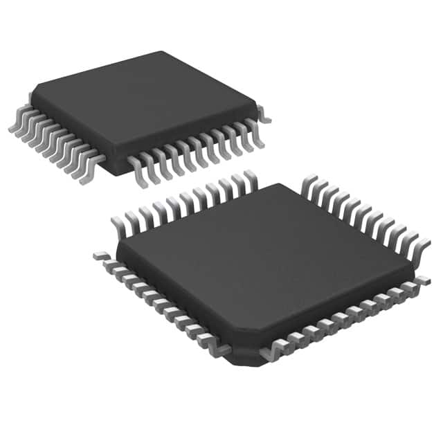
STMicroelectronics TDA7340G
- Part No.:
- TDA7340G
- Manufacturer:
- STMicroelectronics
- Category:
- Audio Special Purpose
- Package:
- 44-QFP
- Datasheet:
-
 TDA7340G.pdf
- Description:
- IC AUDIO SIGNAL PROCESSOR 44PQFP
- Quantity:
- Payment:

- Shipping:

Inventory:3,267
Please send an inquiry. Send us your inquiry, and we will respond immediately.
Product details
Overview
TDA7340G from STMicroelectronics is an I²C-controlled audio signal processor for automotive radio systems, integrating audioprocessor, stereodecoder, noise blanker, pause detector, and multiple mute functions in a single PQFP44 package. It supports differential CD, stereo cassette/FM, mono/stereo AM, telephone, and beep inputs; provides ±14 dB bass/treble control, 37.5 dB independent speaker attenuation, zero-crossing mute (20–160 mV threshold), and integrated 456 kHz VCO with adjustment-free PLL loop filter.
For engineers reviewing the TDA7340G datasheet, TDA7340G pinout, TDA7340G application, or TDA7340G equivalent, key selection considerations include its BICMOS-based low-distortion signal path (0.01% THD), programmable noise blanker trigger thresholds (35–65 mV), stereo blend and high-cut control via analog voltage, and I²C-configurable soft/zero-crossing mute timing - all critical for FM/AM car radio audio integrity and interference suppression.
Technical Context
The TDA7340G implements a fully integrated stereo decoder with automatic pilot-dependent mono/stereo switching, internal 19 kHz pilot cancellation, and 55–95 dB carrier/harmonic suppression (19–190 kHz). Its BICMOS architecture enables CMOS-switched capacitor filters, eliminating external components for the PLL loop filter and pilot detector integrator.
Audio processing uses linear CMOS switching instead of bipolar multipliers, achieving ≤0.08% distortion and ≤5 µV input noise (differential CD input). The noise blanker includes dual-path triggering (field strength, deviation, high-frequency spikes), programmable rectifier thresholds (0.9–3.4 V), and 40 µs suppression pulse duration with <10 pA offset current during hold time.
Key Specifications
| Parameter | Value and Actual Design Meaning |
|---|---|
| Supply Voltage | 6–10 V - compatible with automotive battery range (9 V nominal); max 10.5 V absolute rating |
| Supply Current | 10–25 mA - scales with stereo decoder ON/OFF state; enables low-power mono operation |
| THD+N | 0.01–0.08% - ensures high-fidelity audio reproduction without audible artifacts in car cabin environments |
| Input Noise (CD) | 5 µV - measured 20 Hz–20 kHz flat; enables clean amplification of low-level CD signals |
| S/N Ratio | 106 dB - referenced to 1 VRMS output; supports wide dynamic range for quiet passages and loud transients |
| Channel Separation | 80–100 dB - prevents crosstalk between left/right channels in stereo decoding and processing |
| VCO Frequency | 456 kHz - fixed, adjustment-free oscillator for precise stereo pilot detection and demodulation |
Pinout & Package
PQFP44 (Plastic Quad Flat Package, 44-pin, 10 × 10 mm, 0.8 mm pitch) with exposed thermal pad. Pin mapping validated per STMicroelectronics datasheet revision D94AU055A (page 4/27).
| Pin/Terminal | Circuit Role | Design Meaning |
|---|---|---|
| 1, 2, 3, 5, 6, 4, 7, 8, 9, 10, 17, 11, 18, 19, 20, 21, 22, 44, 43, 42, 41, 39, 40, 38, 37, 36, 35, 34, 28, 27, 26, 24, 23, 25, 33, 32, 31, 29, 30 | GND / Power Ground | Digital and analog ground pins - require separate AGND/DGND routing per layout note 13 to minimize noise coupling |
| 12, 13, 14, 15, 16 | CD L+, CD L−, CD R+, CD R− | Differential CD input pair - supports quasi-diff or full-diff mode; gain programmable in 3.75 dB steps |
| 24, 23 | IN L, IN R | Stereo line-level inputs - for cassette/FM sources; 24–46 kΩ input resistance |
| 31, 30 | AM_L, AM_R | AM mono/stereo inputs - configurable via I²C; includes beep input capability in mono mode |
| 32 | PHONE IN | Differential telephone mono input - 14–26 kΩ resistance; optimized for mobile call integration |
| 29, 28 | OUT LF, OUT LR | Front left speaker outputs - each with independent 1.25 dB step attenuation (0–37.5 dB range) |
| 35, 36 | OUT RF, OUT RR | Rear speaker outputs - identical attenuation control; mute function available per channel |
| 37, 38 | BIN L, BOUT L | Stereo blend control interface - analog voltage (VSB−VR) sets channel separation from 6 dB to 26 dB |
| 39, 40 | HCL, HCR | High-cut control outputs - drive external RC network to adjust de-emphasis time constant (50 µs nominal) |
| 25 | MPX | Composite stereo MPX input - feeds stereodecoder; 35–65 kΩ input resistance, 0.5–1.25 VRMS nominal level |
| 11 | PAUSE | Pause detector output - open-drain, active-low; threshold programmable via external capacitor |
| 41 | MUTE | Direct mute control input - TTL-compatible; triggers 80–100 dB output attenuation |
| 33 | SOFT MUTE | External slope control for soft mute - current-sink pin; defines rise/fall time (0.8–45 ms) |
| 22 | CREF | Reference capacitor pin - connects 10–22 µF capacitor to set internal DC reference level; critical for pop-free power-on |
| 21 | SCL | I²C clock input - supports up to 500 kbit/s; requires pull-up resistor |
| 20 | SDA | I²C data bidirectional - open-drain; acknowledges writes with 0.4–0.8 V low-level |
| 19 | DIGGND | Digital ground - isolated from analog ground to prevent digital switching noise injection |
Key Features
| Feature | Design Value |
|---|---|
| Zero-Crossing Mute | Programmable 20–160 mV threshold ensures mute activation at signal zero-crossings, eliminating audible click/pop |
| Integrated Noise Blanker | 2nd-order high-pass filter + noise rectifier + programmable trigger enables >55 dB impulse noise suppression (e.g., ignition spikes) |
| Independent Speaker Control | Four 1.25 dB-step attenuators (LF/LR/RF/RR) allow precise channel balancing and fade/pan without external DACs |
| Adjustment-Free VCO & PLL | On-chip 456 kHz oscillator and loop filter eliminate 3–5 external components typically required in stereo decoders |
| I²C-Configurable Loudness | Fully programmable 15×1.25 dB loudness curve (−18.75 to 0 dB) compensates for human ear sensitivity at low volumes |
Applications
| FM/AM Car Radio Audio Processing | Multi-Source Automotive Head Unit |
|---|---|
Use Scenario: Integrated audio processor in OEM car radios handling FM stereo MPX demodulation, AM mono decoding, and CD/cassette playback. IC Role / Device Role / Timing Role: Central audio signal conditioner - performs pilot detection, stereo blending, bass/treble shaping, speaker-level attenuation, and noise blanking in real time. Use Value: Eliminates need for discrete op-amps, filters, and VCOs; reduces BOM count by ≥12 passive components while maintaining 91 dB S+N ratio and <0.02% THD. | Use Scenario: Unified audio hub in infotainment systems supporting Bluetooth phone calls, USB audio, and analog aux inputs. IC Role / Device Role / Timing Role: Input multiplexer and volume/loudness engine - selects between differential CD, telephone mono, and stereo line sources with seamless gain matching. Use Value: Enables consistent loudness across sources via I²C-programmable 1.25 dB fine volume steps and 3.75 dB coarse gain stages, reducing DSP load. |
| Automotive Noise Suppression System | High-Fidelity Stereo Decoder Module |
Use Scenario: Mitigating ignition noise, alternator whine, and RF interference in 12 V vehicle electrical environments. IC Role / Device Role / Timing Role: Adaptive noise blanker - detects spikes via LEVEL pin or internal MPX path, triggers 40 µs suppression pulses with field-strength-dependent threshold. Use Value: Achieves >75 dB adjacent-channel interference rejection (114/190 kHz) and 55–90 dB subcarrier suppression without external notch filters. | Use Scenario: High-performance stereo decoding for premium audio systems requiring minimal intermodulation distortion. IC Role / Device Role / Timing Role: Precision stereodecoder - uses BICMOS switched-capacitor filters for pilot cancellation, roll-off compensation, and mono/stereo auto-switching. Use Value: Delivers 65–75 dB intermodulation suppression (α2/α3) and 50 dB channel separation at 100 mVDC imbalance - exceeding EIAJ CP-3100 standards. |
Equivalent & Alternatives
The following parts are listed as comparable options for similar audio signal processor applications.
| Alternative Part | Technical Difference | Application Difference | Selection Advice |
|---|---|---|---|
| TDA7341 | Same pinout and core architecture; adds enhanced I²C error recovery and improved 19 kHz pilot rejection (80 dB vs. 75 dB) | Preferred for new designs requiring higher stereo purity in weak-signal urban reception | Select when pilot signal robustness > cost sensitivity; not drop-in due to revised I²C ACK timing |
| STA559BW | Dual-channel Class-D amplifier + integrated audio processor; lacks dedicated noise blanker and pause detector | Targets compact all-in-one solutions where space constraints preclude discrete audio processors | Choose only if speaker driver integration is mandatory; sacrifices TDA7340G's 4-speaker independent control and zero-crossing mute |
Compared with TDA7340G, TDA7341 improves pilot rejection and I²C reliability but requires firmware updates, while STA559BW trades audio processing depth for power efficiency and board area - making TDA7340G optimal for legacy car radio upgrades needing full feature parity.
Availability
TDA7340G is available at Aetrix Electronics and suitable for automotive infotainment systems, OEM car radio replacements, and high-fidelity stereo decoder modules requiring stable component supply across extended temperature ranges (−40°C to +85°C).
Supply support for TDA7340G includes scheduled delivery planning, volume procurement assistance, BOM continuity management, traceable sourcing, and lifecycle availability coordination for OEM customers, industrial embedded developers, connected-device designers, and electronics production programs.
Manufacturer
STMicroelectronics is a global semiconductor leader headquartered in Geneva, Switzerland, specializing in automotive, industrial, and power management ICs with over 45 years of analog/mixed-signal design heritage.
The TDA7340G belongs to ST's automotive audio processor product line, engineered specifically for cost-sensitive, high-reliability car radio platforms requiring integrated stereo decoding, multi-source mixing, and robust noise immunity in harsh electrical environments.
FAQ
What is the purpose of the CREF pin on the TDA7340G?
The CREF pin connects to an external 10–22 µF capacitor that establishes the internal DC reference voltage (Vs/2) for analog circuitry. This reference stabilizes bias points across the audioprocessor, stereodecoder, and noise blanker blocks. Proper CREF sizing (e.g., 22 µF) ensures pop-free power-on sequencing by controlling the rise time of output pins and preventing transient clicks during startup, as confirmed in datasheet Figure 4–6.
How does the zero-crossing mute function work, and what threshold values are supported?
Zero-crossing mute activates attenuation only when the audio signal crosses 0 V, eliminating switching transients. Threshold is set via I²C bits D6/D5 (WIN): 20 mV (WIN=11), 40 mV (WIN=10), 80 mV (WIN=01), or 160 mV (WIN=00). These values define the window around zero crossing within which mute is triggered - verified in Electrical Characteristics Table (page 5/27) and MUTE register description (page 11/27).
Can the TDA7340G decode SCA (Subsidiary Communications Authorization) subcarriers?
Yes - the TDA7340G's stereodecoder achieves 75 dB suppression of 67 kHz SCA subcarriers (α67), enabling reliable reception of auxiliary services like traffic or weather data. This performance is measured per note 3 in the datasheet (page 8/27) using an 81% mono + 9% pilot + 10% unmodulated 67 kHz test signal, confirming native SCA compatibility without external filtering.
What layout guidelines are critical for minimizing noise in the TDA7340G design?
Per datasheet note 13 (page 9/27), AGND and DGND traces must be physically separated and joined only at a single point near the device. A 50 Ω resistor is recommended on the CD differential lines, placed as far as possible from the IC. Additionally, the CREF capacitor must be placed close to pin 22, and the 1 nF C13/C14 de-emphasis capacitors should be routed with minimal parasitic inductance to maintain 50 µs time constant accuracy.
TDA7340G Specifications
- Product attributes
- Attribute value
- Manufacturer:
- STMicroelectronics
- Series:
- -
- Package/Case:
- 44-QFP
- Packaging:
- Tray
- Product Status:
- Obsolete
- Function:
- Audio Signal Processor
- Applications:
- Audio Systems
- Number of Channels:
- 2
- Interface:
- I2C
- Voltage - Supply:
- 6V ~ 10V
- Operating Temperature:
- -40°C ~ 85°C (TA)
- Specifications:
- -
- Mounting Type:
- Surface Mount
- Grade:
- -
TDA7340G FAQ
1.How can I place an order for TDA7340G through Aetrix?
Please submit a Request for Quotation (RFQ) for TDA7340G on Aetrix. Our sales agent will provide a competitive quotation and guide you through the order confirmation once you accept the terms.
2.Are the price and stock information for TDA7340G reliable?
The price and inventory of TDA7340G are updated periodically and may fluctuate due to market conditions. Stock and pricing data are typically refreshed every 24 hours. Quotation validity for TDA7340G is usually 5 days.
3.What payment methods are accepted for TDA7340G?
We accept Wire Transfer, PayPal, Credit Card, Western Union, MoneyGram, and Escrow for TDA7340G transactions.
Note: Certain payment methods may incur a processing fee.
4.How is shipping managed for TDA7340G?
TDA7340G orders can be shipped via leading logistics carriers, including DHL, UPS, FedEx, TNT, or Registered Mail.
Once your TDA7340G order is processed, you will receive an email with the shipment details and tracking number.
Note: Tracking information may take up to 24 hours to appear. Express delivery typically takes 3–5 business days.
5.How can I obtain technical support or documentation for TDA7340G?
For technical support, including TDA7340G datasheets, pinout diagrams, or application guidance, please contact our engineering support team. They can provide detailed documentation and assistance for your TDA7340G requirements.
6.How does Aetrix verify that TDA7340G is sourced from the original manufacturer or authorized distributors?
All TDA7340G products on Aetrix are procured from qualified distributors and authorized channels. Our dedicated quality assurance team conducts strict verification, including traceability checks and, if necessary, third-party testing. This ensures that TDA7340G meets industry standards.
7.What is the process for return or replacement of TDA7340G?
All TDA7340G units undergo pre-shipment inspection (PSI). If there is an issue with TDA7340G, returns or replacements are accepted under the following conditions:
1.Quantity discrepancies, incorrect items, or visible external defects (such as breakage or corrosion), acknowledged by Aetrix.
2.The issue is reported within 90 days of delivery.
3.The TDA7340G part is unused and in its original packaging.
Return procedure for TDA7340G:
1.Submit a request within 90 days.
2.Obtain a Return Material Authorization (RMA) from Aetrix.
TDA7340G Tags

-
SA571DR2G
onsemi
-
ADAU7002ACBZ-R7
Analog Devices Inc.

-
DRV135UA/2K5
Texas Instruments

-
DRV134UA/1K
Texas Instruments

-
DRV134PA
Texas Instruments
-
DRV134UA
Texas Instruments
-
DRV135UA
Texas Instruments
-
SA572DR2G
onsemi
-
PGA2311U/1K
Texas Instruments
-
SI8244BB-D-IS1R
Skyworks Solutions Inc.

-
CS8416K-CZZR
Cirrus Logic Inc.
-
SRC4392IPFBR
Texas Instruments
Tech Hub

A practical engineering guide to 3.3V and 5V logic compatibility, input thresholds, resistor dividers, translator ICs, MOSFET level shifting, I2C pull-ups, timing limits and power-sequencing risks.

The 74HC595 uses push-pull logic outputs, while the TPIC6B595 uses 50 V open-drain DMOS sinks for higher-power loads. This guide compares timing, current limits, 3.3 V interfacing, load wiring, thermal…

The 74HC595 converts serial data into eight stable parallel outputs. This guide covers pin functions, shift and storage timing, OE and MR behavior, drive-current limits, cascading, voltage compatibilit…

A technical comparison of level-sensitive latches and edge-triggered flip-flops, covering timing windows, setup and hold limits, master–slave operation, time borrowing, race-through, HDL inference and…

A D latch stores one bit while Enable controls when data can pass. This reference covers gate-level operation, truth tables, transparency, setup and hold timing, LE versus OE, common ICs and practical …

An SR latch stores one bit through cross-coupled feedback. This engineering reference covers NOR and NAND implementations, truth tables, forbidden-state recovery, gated operation, switch debouncing, fa…

Latch circuits retain one bit through feedback. This technical reference covers SR and D latches, truth tables, transparency, timing limits, latch-versus-flip-flop behavior, applications and common log…

An engineering guide to LED driver operation, constant-current and constant-voltage outputs, linear and switching topologies, dimming, IC selection, calculations, replacement compatibility, and fault c…

Operational amplifier guide covering op amp basics, feedback, ideal vs real op amps, common configurations, buffer circuits, offset, bias current, gain-bandwidth, slew rate, rail-to-rail limits and sel…

Jumper cables guide covering safe connection order, red and black clamp placement, final ground connection, cable gauge, length, clamp quality, copper vs CCA cables, jump starter comparison and battery…


