
 My Inquiry
 My Account


STMicroelectronics TDA7440D
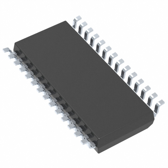
- Part No.:
- TDA7440D
- Manufacturer:
- STMicroelectronics
- Category:
- Audio Special Purpose
- Package:
- 28-SOIC (0.295", 7.50mm Width)
- Datasheet:
-
 TDA7440D.pdf
- Description:
- IC AUDIO TONE PROCESSOR 28SO
- Quantity:
- Payment:

- Shipping:

Inventory:4,680
Please send an inquiry. Send us your inquiry, and we will respond immediately.
Product details
Overview
TDA7440D from STMicroelectronics is a digitally controlled stereo audio processor IC for Hi-Fi systems, integrating 4-channel stereo input multiplexing, programmable bass/treble (±14 dB in 2 dB steps), volume control (−47 dB to 0 dB in 1 dB steps), independent left/right speaker attenuation (−79 dB mute), and I²C serial bus interface. It operates from 6–10.2 V supply and delivers <0.08% THD at 1 kHz with 106 dB signal-to-noise ratio.
For engineers reviewing the TDA7440D datasheet, TDA7440D pinout, TDA7440D application, or TDA7440D equivalent, this device serves as a complete analog front-end tone/volume/balance processor requiring no external microcontroller for basic operation-ideal for legacy AV receivers, integrated amplifiers, and multi-source audio hubs where low-noise analog signal path integrity and precise digital control coexist.
Technical Context
The TDA7440D implements a bipolar/CMOS hybrid architecture with resistor-network-based gain switching and op-amp signal conditioning, enabling DC-free stepping and low distortion (<0.01% typ. THD). Its I²C interface supports both incremental and non-incremental byte writes, with dedicated subaddress mapping for input selection, gain, volume, bass, treble, and speaker attenuation registers.
All analog signal paths-including input multiplexer, bass/treble filters, and speaker attenuators-are fully decoupled and independently controllable via 8-bit register writes. External component selection (e.g., CREF = 10 µF, RB = 44 kΩ) sets bass center frequency and treble time constant, allowing system-level tuning of tonal response without firmware changes.
Key Specifications
| Parameter | Value and Actual Design Meaning |
|---|---|
| Supply Voltage | 6–10.2 V - Supports standard 9 V rail; stable operation down to 5 V with functional retention |
| THD+N | 0.01–0.08% @ 1 kHz, 1 Vrms - Ensures audibly transparent signal path in high-fidelity playback |
| S/N Ratio | 95–106 dB - Achieved with internal 20 µA bias current design minimizing thermal noise contribution |
| Channel Separation | 80–100 dB @ 1 kHz - Maintains stereo imaging fidelity across full control range |
| Volume Control Range | −47 dB to 0 dB in 1 dB steps - Enables fine-grained loudness matching without audible "zipper" noise |
| Bass/Treble Range | ±14 dB in 2 dB steps - Provides discrete, repeatable tonal shaping aligned with psychoacoustic perception thresholds |
| Mute Attenuation | 80–100 dB - Fully silences output without relay switching or power cycling |
Pinout & Package
SO-28 surface-mount package (17.7–18.1 mm × 10–10.65 mm, 1.27 mm pitch), RoHS-compliant ECOPACK® variant.
| Pin/Terminal | Circuit Role | Design Meaning |
|---|---|---|
| 1–7, 28 | L/R Input Channels (IN1–IN4) | Four stereo input pairs accept line-level signals; selectable via I²C register |
| 8, 9 | Bass IN/OUT (L/R) | External RC network defines bass center frequency and Q factor per channel |
| 10, 11 | Treble IN/OUT (L/R) | Internal 25 kΩ resistor + external capacitor set treble cutoff frequency |
| 12, 14 | Speaker Attenuator L/R Output | Digitally controlled 1 dB-step attenuators feed speaker-level outputs directly |
| 13, 15 | Audio Outputs (LOUT/ROUT) | Main stereo outputs with 10–30 Ω impedance; compatible with 2 kΩ minimum load |
| 18, 19 | I²C Bus (SDA/SCL) | Open-drain bidirectional interface; requires external pull-ups to VS |
| 20 | DIG_GND | Digital ground reference isolated from analog ground (AGND, Pin 21) to prevent coupling |
| 21 | AGND | Analog ground return for all signal paths; must be star-connected to minimize noise |
| 22, 23 | Bass/Treble Feedback (BIN/OUT L/R) | Return nodes for external filter networks; define gain and frequency response |
| 24–27 | Power & Reference (VS, CREF, VREF) | VS = main supply; CREF = 10 µF decoupling for internal reference stability; VREF = buffered reference |
Key Features
| Feature | Design Value |
|---|---|
| 4× Stereo Input Multiplexer | Selects among four independent line sources with programmable 0–30 dB input gain per channel |
| Independent Speaker Attenuation | Left/right channels attenuated separately up to −79 dB with 1 dB resolution and mute |
| DC-Step-Free Volume Control | Zero-crossing detection not required; 1 dB steps produce no audible pop/click during adjustment |
| Externally Tunable Tone Filters | Bass center frequency and treble cutoff set by user-selected R/C components-not fixed internally |
| I²C Register Map with Auto-Increment | Enables burst writes to consecutive function registers (volume → bass → treble) in single transaction |
Applications
| Home Audio Receiver | Integrated Stereo Amplifier |
|---|---|
|
Use Scenario: Multi-source AV receiver switching between CD, tuner, phono, and auxiliary inputs while preserving tonal balance across sources. IC Role / Device Role / Timing Role: Central analog signal router and tone processor-handles input selection, gain normalization, and real-time bass/treble/volume adjustment. Use Value: Eliminates need for discrete op-amp gain stages and mechanical potentiometers; enables remote-controlled, repeatable sound signature recall. |
Use Scenario: Compact stereo amplifier with front-panel digital controls and memory presets for volume, tone, and source. IC Role / Device Role / Timing Role: Analog signal conditioner and digital control interface-accepts I²C commands from MCU and drives power amp inputs. Use Value: Reduces BOM count by >12 passive components vs. discrete solution; maintains <0.08% THD across full 47 dB volume range. |
| Professional Studio Monitor Controller | Automotive Aftermarket Head Unit |
|
Use Scenario: Reference-grade monitor controller routing D/A converter outputs to multiple speaker pairs with independent level/tone per zone. IC Role / Device Role / Timing Role: Precision analog signal manager-provides calibrated attenuation, channel balance, and tonal correction before power amplification. Use Value: Delivers 106 dB S/N and 90 dB channel separation, meeting EBU R68 monitoring standards without external buffering. |
Use Scenario: High-end car head unit supporting Bluetooth, USB, and FM with adaptive loudness compensation and cabin EQ. IC Role / Device Role / Timing Role: Audio preprocessing engine-normalizes input levels from varied sources and applies vehicle-specific bass boost profiles. Use Value: Enables factory-tuned EQ curves stored in MCU flash and applied via I²C; handles 10.5 V automotive supply transients robustly. |
Equivalent & Alternatives
The following parts are listed as comparable options for similar stereo audio processor applications.
| Alternative Part | Technical Difference | Application Difference | Selection Advice |
|---|---|---|---|
| CS4272-CQZ | 24-bit DAC + DSP core; requires external microcontroller for tone control logic; higher SNR (110 dB) but no integrated input mux | Best for designs needing embedded digital filtering and sample-rate conversion-not pure analog signal conditioning | Choose when migrating to digital audio domain; avoid if retaining analog front-end simplicity is critical |
| PGA2310UA | Analog volume/balance IC only; no tone control, no input mux, no I²C-uses analog voltage or SPI interface | Suitable for ultra-low-noise preamp stages where tone processing is handled externally | Choose only if tone control is implemented upstream; incompatible with TDA7440D's integrated feature set |
Compared with CS4272-CQZ and PGA2310UA, the TDA7440D uniquely integrates input multiplexing, tone control, speaker attenuation, and I²C interface in a single analog-centric IC-eliminating external logic while maintaining <0.08% THD and 106 dB SNR without requiring DAC or DSP resources.
Availability
TDA7440D is available at Aetrix Electronics and suitable for home audio receivers, integrated stereo amplifiers, professional monitor controllers, and automotive aftermarket head units requiring stable component supply and long-term obsolescence management.
Supply support for TDA7440D includes scheduled delivery planning, volume procurement assistance, BOM continuity management, traceable sourcing, and lifecycle availability coordination for OEM customers, industrial embedded developers, connected-device designers, and electronics production programs.
Manufacturer
STMicroelectronics is a global semiconductor leader headquartered in Geneva, Switzerland, designing and manufacturing analog, mixed-signal, and power ICs for industrial, automotive, and consumer markets.
The TDA7440D belongs to ST's legacy audio processor family targeting high-fidelity analog signal conditioning-designed specifically for cost-sensitive, high-SNR audio systems where digital control must coexist with pristine analog performance.
FAQ
What is the minimum supply voltage for reliable I²C communication on the TDA7440D?
The TDA7440D maintains full I²C functionality-including address recognition, data acknowledge, and register write execution-down to 5 V supply. Electrical characteristics tables confirm stable operation at VS = 5 V, though the absolute maximum rating specifies 10.5 V and typical operation occurs at 9 V. No reset occurs during step-down from 9 V to 4 V, ensuring robust bus recovery.
How does the TDA7440D achieve zero-crossing–free volume control without microcontroller intervention?
It uses internal analog switch matrices and precision resistor ladders controlled by decoded I²C register bits-not PWM or digital interpolation. Each 1 dB step corresponds to a physical tap change in a monolithic thin-film resistor network, eliminating switching transients. The bipolar/CMOS process ensures <0.5 mV DC offset between steps, preventing audible clicks even during rapid adjustments.
Can the bass and treble center frequencies be modified after PCB layout?
Yes-both are set by external passive components: bass stage uses user-selected R and C values on BIN/BOUT pins to define center frequency (Fc), Q factor, and gain; treble stage relies on an external capacitor to ground from TREBLE(L/R) pins, with internal 25 kΩ resistor fixing the time constant. No re-spin is needed to tune response.
Is the TDA7440D pin-compatible with any newer ST audio processors?
No direct pin-compatible successor exists. ST discontinued the TDA7440D in favor of digital audio SoCs (e.g., STA3xx series) with integrated DSP and Class-D drivers. The SO-28 footprint, I²C register map, and analog signal routing are unique to this generation; migration requires PCB redesign and firmware adaptation to new command structures.
TDA7440D Specifications
- Product attributes
- Attribute value
- Manufacturer:
- STMicroelectronics
- Series:
- -
- Package/Case:
- 28-SOIC (0.295", 7.50mm Width)
- Packaging:
- Tube
- Product Status:
- Obsolete
- Function:
- Audio Tone Processor
- Applications:
- Consumer Audio
- Number of Channels:
- 2
- Interface:
- I2C
- Voltage - Supply:
- 6V ~ 10.2V
- Operating Temperature:
- 0°C ~ 70°C (TA)
- Specifications:
- -
- Mounting Type:
- Surface Mount
- Grade:
- -
TDA7440D FAQ
1.How can I place an order for TDA7440D through Aetrix?
Please submit a Request for Quotation (RFQ) for TDA7440D on Aetrix. Our sales agent will provide a competitive quotation and guide you through the order confirmation once you accept the terms.
2.Are the price and stock information for TDA7440D reliable?
The price and inventory of TDA7440D are updated periodically and may fluctuate due to market conditions. Stock and pricing data are typically refreshed every 24 hours. Quotation validity for TDA7440D is usually 5 days.
3.What payment methods are accepted for TDA7440D?
We accept Wire Transfer, PayPal, Credit Card, Western Union, MoneyGram, and Escrow for TDA7440D transactions.
Note: Certain payment methods may incur a processing fee.
4.How is shipping managed for TDA7440D?
TDA7440D orders can be shipped via leading logistics carriers, including DHL, UPS, FedEx, TNT, or Registered Mail.
Once your TDA7440D order is processed, you will receive an email with the shipment details and tracking number.
Note: Tracking information may take up to 24 hours to appear. Express delivery typically takes 3–5 business days.
5.How can I obtain technical support or documentation for TDA7440D?
For technical support, including TDA7440D datasheets, pinout diagrams, or application guidance, please contact our engineering support team. They can provide detailed documentation and assistance for your TDA7440D requirements.
6.How does Aetrix verify that TDA7440D is sourced from the original manufacturer or authorized distributors?
All TDA7440D products on Aetrix are procured from qualified distributors and authorized channels. Our dedicated quality assurance team conducts strict verification, including traceability checks and, if necessary, third-party testing. This ensures that TDA7440D meets industry standards.
7.What is the process for return or replacement of TDA7440D?
All TDA7440D units undergo pre-shipment inspection (PSI). If there is an issue with TDA7440D, returns or replacements are accepted under the following conditions:
1.Quantity discrepancies, incorrect items, or visible external defects (such as breakage or corrosion), acknowledged by Aetrix.
2.The issue is reported within 90 days of delivery.
3.The TDA7440D part is unused and in its original packaging.
Return procedure for TDA7440D:
1.Submit a request within 90 days.
2.Obtain a Return Material Authorization (RMA) from Aetrix.
TDA7440D Tags

-
SA571DR2G
onsemi
-
ADAU7002ACBZ-R7
Analog Devices Inc.

-
DRV135UA/2K5
Texas Instruments

-
DRV134UA/1K
Texas Instruments

-
DRV134PA
Texas Instruments
-
DRV134UA
Texas Instruments
-
DRV135UA
Texas Instruments
-
SA572DR2G
onsemi
-
PGA2311U/1K
Texas Instruments
-
SI8244BB-D-IS1R
Skyworks Solutions Inc.

-
CS8416K-CZZR
Cirrus Logic Inc.
-
SRC4392IPFBR
Texas Instruments
Tech Hub

A practical engineering and sourcing framework covering lifecycle verification, lifetime-buy calculations, replacement qualification, supplier checks and counterfeit-risk controls.

TTL and CMOS logic families differ in thresholds, loading, output drive, power and timing. This engineering guide compares 74HC and 74HCT, calculates noise margins and checks 3.3 V/5 V compatibility.

A practical engineering guide to 3.3V and 5V logic compatibility, input thresholds, resistor dividers, translator ICs, MOSFET level shifting, I2C pull-ups, timing limits and power-sequencing risks.

The 74HC595 uses push-pull logic outputs, while the TPIC6B595 uses 50 V open-drain DMOS sinks for higher-power loads. This guide compares timing, current limits, 3.3 V interfacing, load wiring, thermal…

The 74HC595 converts serial data into eight stable parallel outputs. This guide covers pin functions, shift and storage timing, OE and MR behavior, drive-current limits, cascading, voltage compatibilit…

A technical comparison of level-sensitive latches and edge-triggered flip-flops, covering timing windows, setup and hold limits, master–slave operation, time borrowing, race-through, HDL inference and…

A D latch stores one bit while Enable controls when data can pass. This reference covers gate-level operation, truth tables, transparency, setup and hold timing, LE versus OE, common ICs and practical …

An SR latch stores one bit through cross-coupled feedback. This engineering reference covers NOR and NAND implementations, truth tables, forbidden-state recovery, gated operation, switch debouncing, fa…

Latch circuits retain one bit through feedback. This technical reference covers SR and D latches, truth tables, transparency, timing limits, latch-versus-flip-flop behavior, applications and common log…

An engineering guide to LED driver operation, constant-current and constant-voltage outputs, linear and switching topologies, dimming, IC selection, calculations, replacement compatibility, and fault c…


