
 My Inquiry
 My Account


STMicroelectronics TDA7449
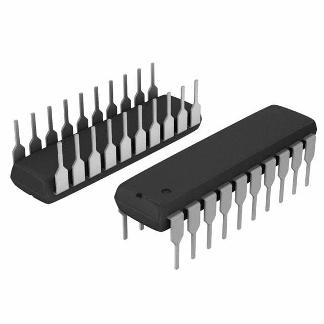
- Part No.:
- TDA7449
- Manufacturer:
- STMicroelectronics
- Category:
- Audio Special Purpose
- Package:
- 20-DIP (0.300", 7.62mm)
- Datasheet:
-
 TDA7449.pdf
- Description:
- IC VOLUME CONTROL 20DIP
- Quantity:
- Payment:

- Shipping:

Inventory:4,610
Please send an inquiry. Send us your inquiry, and we will respond immediately.
Product details
Overview
TDA7449 from STMicroelectronics is a digitally controlled stereo audio processor IC for TV system tone, volume, balance, and speaker attenuation functions. It features dual-band (bass/treble) tone control in 2 dB steps, volume control in 1 dB steps, two independent 1 dB-step speaker attenuators with mute, and selectable input gain up to +30 dB. It operates from 6–10.2 V supply and delivers <0.08% THD at 1 VRMS output.
For engineers reviewing the TDA7449 datasheet, TDA7449 pinout, TDA7449 application, or TDA7449 equivalent, this device is selected for precision analog audio signal conditioning in consumer TV audio subsystems where I²C-programmable gain, filtering, and channel balancing are required without external DACs or op-amp networks.
Technical Context
The TDA7449 integrates bipolar/CMOS technology to achieve low distortion (<0.08% THD), high signal-to-noise ratio (106 dB), and minimal DC stepping (≤3 mV). Its internal resistor networks and operational amplifiers implement AC signal processing without digital-to-analog conversion.
It uses a 2-wire I²C interface (SCL/SDA) for register-based control of all functions-including input multiplexing, treble/bass filters with externally configurable center frequency and Q factor, and dual independent speaker attenuators. The device supports both incremental and non-incremental bus protocols with 8-bit subaddressing.
Key Specifications
| Parameter | Value and Actual Design Meaning |
|---|---|
| Supply Voltage | 6–10.2 V - Enables direct use with standard 9 V TV power rails; functional down to 5 V per note. |
| THD+N | 0.01–0.08% @ 1 kHz, 1 VRMS - Ensures transparent audio reproduction without audible coloration. |
| Signal-to-Noise Ratio | 106 dB - Supports high-fidelity output even at low volume settings. |
| Tone Control Resolution | Bass/treble: ±14 dB in 2 dB steps - Provides precise, repeatable tonal shaping across full range. |
| Volume Control Range | −47 dB to 0 dB in 1 dB steps - Enables fine-grained loudness matching and mute (100 dB attenuation). |
| Input Gain Range | 0–30 dB in 2 dB steps - Allows optimal level matching between diverse analog sources (e.g., tuner vs. HDMI audio DAC). |
| Channel Separation | 90 dB @ 1 kHz - Maintains stereo imaging integrity during balance and attenuation adjustments. |
Pinout & Package
The TDA7449 is housed in a 20-pin Small Outline (SO20) package with 1.27 mm pitch, compliant with ECOPACK® environmental standards.
| Pin/Terminal | Circuit Role | Design Meaning |
|---|---|---|
| 1, 3, 4, 5, 6, 7, 8, 9 | Stereo Input Terminals | L-IN1/R-IN1, L-IN2/R-IN2, BIN(L)/BIN(R), MUXOUT(L)/MUXOUT(R) - Support dual stereo inputs and internal multiplexer routing. |
| 10, 11 | Audio Outputs | LOUT, ROUT - Buffered line-level outputs capable of driving 2 kΩ loads with ≤2.6 VRMS clipping. |
| 12, 15 | Speaker Attenuator Outputs | BOUT(L), BOUT(R) - Dedicated buffered outputs for speaker-level attenuation with independent mute control. |
| 13, 14 | Treble Filter Pins | TREBLE(L), TREBLE(R) - Connect external capacitors to set high-pass filter corner frequency and response shape. |
| 16, 17 | I²C Interface | SCL, SDA - Bidirectional 2-wire serial bus for configuration; requires external pull-up resistors. |
| 18, 19, 20 | Power & Reference | DIG_GND, CREF, VS - Separate digital ground, 10 μF reference capacitor node, and main supply (6–10.2 V). |
Key Features
| Feature | Design Value |
|---|---|
| Dual independent speaker attenuators | 0 to −79 dB in 1 dB steps per channel, with dedicated mute - Enables precise left/right speaker level trimming without affecting main audio path. |
| Externally configurable bass/treble filters | Center frequency and Q factor set via external R/C on BASS/ TREBLE pins - Allows optimization for speaker response or room acoustics. |
| Input multiplexer with programmable gain | Two stereo inputs selectable via I²C; gain adjustable from 0 to +30 dB in 2 dB steps - Simplifies source switching and level normalization in multi-input TVs. |
| Low-noise analog signal path | 106 dB SNR, 90 dB channel separation, <0.08% THD - Delivers studio-grade audio fidelity without requiring post-processing compensation. |
| I²C-compatible control interface | Standard 2-wire protocol with auto-increment mode and 8-bit subaddressing - Reduces MCU GPIO count and simplifies firmware integration. |
Applications
| TV Audio Subsystem | Set-Top Box Audio Processing |
|---|---|
|
Use Scenario: Integrated audio signal conditioning in CRT/LCD/LED television mainboards handling tuner, HDMI, and auxiliary analog inputs. IC Role / Device Role / Timing Role: Central analog audio processor managing input selection, volume, tone, balance, and speaker drive level before final amplification. Use Value: Eliminates discrete op-amp networks and manual trimmers; enables factory calibration and user-adjustable EQ via remote control MCU. |
Use Scenario: Audio preprocessing in digital cable/satellite receivers where multiple decoded audio streams require consistent analog output levels and tonal character. IC Role / Device Role / Timing Role: Post-decoder analog conditioning block performing gain normalization, bass/treble enhancement, and stereo balance correction. Use Value: Maintains uniform loudness and spectral balance across broadcast, streaming, and local media sources without software DSP overhead. |
| Home Theater Soundbar Front-End | Professional Monitor Audio Calibration |
|
Use Scenario: Compact soundbar designs requiring high-fidelity analog signal routing and real-time tone adjustment without digital audio path latency. IC Role / Device Role / Timing Role: Analog domain tone/volume controller interfacing between DAC output and Class-D amplifier inputs. Use Value: Preserves transient integrity and phase coherence while enabling remote-controlled bass boost or treble lift for room-specific tuning. |
Use Scenario: Calibration-grade audio test equipment needing stable, repeatable analog gain and filtering for reference speaker verification. IC Role / Device Role / Timing Role: Precision programmable attenuator and tone shaper used in automated speaker response measurement fixtures. Use Value: Provides traceable, stepwise 1 dB volume and 2 dB tone adjustments with <3 mV DC offset - critical for metrology-grade repeatability. |
Equivalent & Alternatives
The following parts are listed as comparable options for similar stereo audio processor applications.
| Alternative Part | Technical Difference | Application Difference | Selection Advice |
|---|---|---|---|
| TDA7439 | Single-ended inputs only; no speaker attenuators; bass/treble in 1.5 dB steps; 16-pin SOIC package. | Lacks independent speaker-level control and dual input multiplexing - suitable only for simpler audio paths without speaker trimming. | Select when board space is constrained and speaker attenuation is handled externally. |
| CS4272-CZZ | Delta-sigma DAC + analog output stage; I²S/SPDIF interface; integrated headphone amp; requires external microcontroller for tone control. | Replaces analog signal chain with digital audio interface - shifts tone processing to firmware, increasing design complexity but enabling dynamic EQ. | Select when migrating to digital audio architecture and firmware-based audio customization is preferred. |
Compared with TDA7449, TDA7439 offers reduced feature set and smaller footprint but sacrifices speaker-level attenuation and dual-input flexibility; CS4272-CZZ replaces analog programmability with digital audio interface and embedded DAC, requiring significant firmware investment but enabling adaptive audio processing.
Availability
TDA7449 is available at Aetrix Electronics and suitable for TV audio subsystems, set-top box signal conditioning, and professional audio calibration equipment requiring stable component supply and long-term production continuity.
Supply support for TDA7449 includes scheduled delivery planning, volume procurement assistance, BOM continuity management, traceable sourcing, and lifecycle availability coordination for OEM customers, industrial embedded developers, connected-device designers, and electronics production programs.
Manufacturer
STMicroelectronics is a global semiconductor leader headquartered in Geneva, Switzerland, designing and manufacturing analog, mixed-signal, power, and microcontroller solutions for industrial, automotive, and consumer markets.
The TDA7449 belongs to ST's legacy audio processor product line, engineered specifically for high-fidelity analog audio signal conditioning in cost-sensitive, high-volume TV and home entertainment systems.
FAQ
What is the minimum supply voltage required for reliable operation of the TDA7449?
The TDA7449 operates reliably from 6 V to 10.2 V, with functional behavior confirmed down to 5 V per datasheet note. However, full specification compliance-including THD, SNR, and control range-is guaranteed only within the 6–10.2 V range. Operation below 6 V may reduce headroom and increase distortion.
Can the TDA7449 be used with a 3.3 V I²C master microcontroller?
Yes-the TDA7449's SCL and SDA pins accept VIH ≥ 3 V and VIL ≤ 1 V, making them compatible with standard 3.3 V logic. Pull-up resistors must connect to the 3.3 V I²C bus rail, not the 9 V VS supply, to avoid damaging the microcontroller I/O pins.
How is the bass and treble center frequency determined in the TDA7449?
Bass center frequency and Q factor are set by external R/C networks connected between BASS IN/OUT pins; treble corner frequency is set by an external capacitor from TREBLE(L/R) to ground. Internal 25 kΩ resistors define time constants-design equations are provided in Section 3.1 and 3.2 of the datasheet.
Does the TDA7449 include built-in protection against pop/click noise during power-up or mute transitions?
Yes-the device uses bipolar/CMOS process technology to minimize DC stepping (<3 mV between adjacent attenuation steps) and incorporates internal circuitry that suppresses transients during mute activation and volume changes, eliminating audible pop/click artifacts in properly decoupled designs.
TDA7449 Specifications
- Product attributes
- Attribute value
- Manufacturer:
- STMicroelectronics
- Series:
- -
- Package/Case:
- 20-DIP (0.300", 7.62mm)
- Packaging:
- Tube
- Product Status:
- Obsolete
- Function:
- Volume Control
- Applications:
- Consumer Audio
- Number of Channels:
- 2
- Interface:
- I2C
- Voltage - Supply:
- 6V ~ 10.2V
- Operating Temperature:
- 0°C ~ 70°C (TA)
- Specifications:
- 100dB
- Mounting Type:
- Through Hole
- Grade:
- -
TDA7449 FAQ
1.How can I place an order for TDA7449 through Aetrix?
Please submit a Request for Quotation (RFQ) for TDA7449 on Aetrix. Our sales agent will provide a competitive quotation and guide you through the order confirmation once you accept the terms.
2.Are the price and stock information for TDA7449 reliable?
The price and inventory of TDA7449 are updated periodically and may fluctuate due to market conditions. Stock and pricing data are typically refreshed every 24 hours. Quotation validity for TDA7449 is usually 5 days.
3.What payment methods are accepted for TDA7449?
We accept Wire Transfer, PayPal, Credit Card, Western Union, MoneyGram, and Escrow for TDA7449 transactions.
Note: Certain payment methods may incur a processing fee.
4.How is shipping managed for TDA7449?
TDA7449 orders can be shipped via leading logistics carriers, including DHL, UPS, FedEx, TNT, or Registered Mail.
Once your TDA7449 order is processed, you will receive an email with the shipment details and tracking number.
Note: Tracking information may take up to 24 hours to appear. Express delivery typically takes 3–5 business days.
5.How can I obtain technical support or documentation for TDA7449?
For technical support, including TDA7449 datasheets, pinout diagrams, or application guidance, please contact our engineering support team. They can provide detailed documentation and assistance for your TDA7449 requirements.
6.How does Aetrix verify that TDA7449 is sourced from the original manufacturer or authorized distributors?
All TDA7449 products on Aetrix are procured from qualified distributors and authorized channels. Our dedicated quality assurance team conducts strict verification, including traceability checks and, if necessary, third-party testing. This ensures that TDA7449 meets industry standards.
7.What is the process for return or replacement of TDA7449?
All TDA7449 units undergo pre-shipment inspection (PSI). If there is an issue with TDA7449, returns or replacements are accepted under the following conditions:
1.Quantity discrepancies, incorrect items, or visible external defects (such as breakage or corrosion), acknowledged by Aetrix.
2.The issue is reported within 90 days of delivery.
3.The TDA7449 part is unused and in its original packaging.
Return procedure for TDA7449:
1.Submit a request within 90 days.
2.Obtain a Return Material Authorization (RMA) from Aetrix.
TDA7449 Tags

-
SA571DR2G
onsemi
-
ADAU7002ACBZ-R7
Analog Devices Inc.

-
DRV135UA/2K5
Texas Instruments

-
DRV134UA/1K
Texas Instruments

-
DRV134PA
Texas Instruments
-
DRV134UA
Texas Instruments
-
DRV135UA
Texas Instruments
-
SA572DR2G
onsemi
-
PGA2311U/1K
Texas Instruments
-
SI8244BB-D-IS1R
Skyworks Solutions Inc.

-
CS8416K-CZZR
Cirrus Logic Inc.
-
SRC4392IPFBR
Texas Instruments
Tech Hub

A practical engineering and sourcing framework covering lifecycle verification, lifetime-buy calculations, replacement qualification, supplier checks and counterfeit-risk controls.

TTL and CMOS logic families differ in thresholds, loading, output drive, power and timing. This engineering guide compares 74HC and 74HCT, calculates noise margins and checks 3.3 V/5 V compatibility.

A practical engineering guide to 3.3V and 5V logic compatibility, input thresholds, resistor dividers, translator ICs, MOSFET level shifting, I2C pull-ups, timing limits and power-sequencing risks.

The 74HC595 uses push-pull logic outputs, while the TPIC6B595 uses 50 V open-drain DMOS sinks for higher-power loads. This guide compares timing, current limits, 3.3 V interfacing, load wiring, thermal…

The 74HC595 converts serial data into eight stable parallel outputs. This guide covers pin functions, shift and storage timing, OE and MR behavior, drive-current limits, cascading, voltage compatibilit…

A technical comparison of level-sensitive latches and edge-triggered flip-flops, covering timing windows, setup and hold limits, master–slave operation, time borrowing, race-through, HDL inference and…

A D latch stores one bit while Enable controls when data can pass. This reference covers gate-level operation, truth tables, transparency, setup and hold timing, LE versus OE, common ICs and practical …

An SR latch stores one bit through cross-coupled feedback. This engineering reference covers NOR and NAND implementations, truth tables, forbidden-state recovery, gated operation, switch debouncing, fa…

Latch circuits retain one bit through feedback. This technical reference covers SR and D latches, truth tables, transparency, timing limits, latch-versus-flip-flop behavior, applications and common log…

An engineering guide to LED driver operation, constant-current and constant-voltage outputs, linear and switching topologies, dimming, IC selection, calculations, replacement compatibility, and fault c…


