
 My Inquiry
 My Account


STMicroelectronics TDA7502
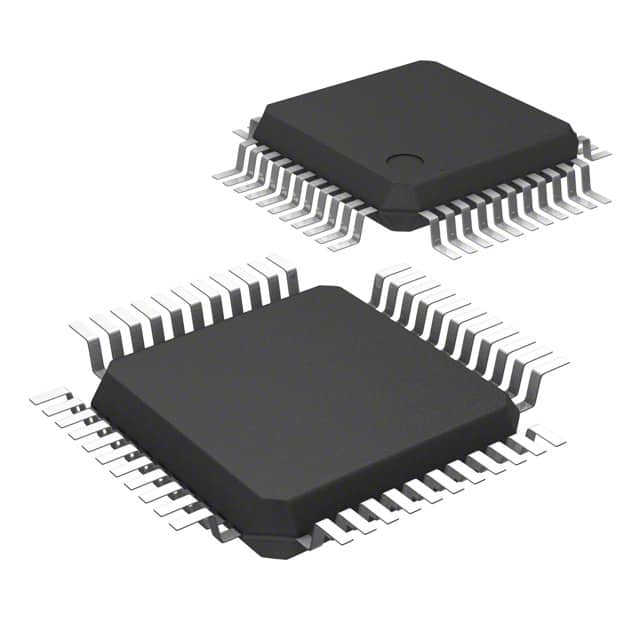
- Part No.:
- TDA7502
- Manufacturer:
- STMicroelectronics
- Category:
- DSP (Digital Signal Processors)
- Package:
- 44-LQFP
- Datasheet:
-
 TDA7502.pdf
- Description:
- IC DSP IN-CAR REMOTE AMP 44-LQFP
- Quantity:
- Payment:

- Shipping:

Inventory:1,347
Please send an inquiry. Send us your inquiry, and we will respond immediately.
Product details
Overview
TDA7502 from STMicroelectronics is a 24-bit fixed-point DSP IC designed for in-car remote amplifier audio processing, featuring a 50 MIPS core, 2×1024×24-bit X/Y data RAM, 3072×24-bit program RAM usable for acoustic delay, serial audio interface (SAI), SPI/I²C master/slave control interfaces, and integrated PLL clock oscillator. It enables parametric equalization, crossover filtering, dynamic compression, and stereo spatial enhancement in automotive head units and OEM amplifier modules.
For engineers reviewing the TDA7502 datasheet, TDA7502 pinout, TDA7502 application, or TDA7502 equivalent, this device is selected for high-fidelity real-time audio signal conditioning where deterministic latency, multi-channel SAI I/O, on-chip delay memory, and 5V-tolerant 3.3V GPIOs are required in cost-sensitive automotive infotainment systems.
Technical Context
The TDA7502 integrates a 24-bit Harvard-architecture DSP core with dual 56-bit accumulators, single-cycle MAC, convergent rounding, and programmable interrupt priorities - enabling deterministic execution of audio algorithms at up to 50 MHz. Its memory architecture includes separate X-RAM, Y-RAM, and 3072-word program RAM, allowing simultaneous data buffering and instruction fetch for low-latency FIR/IIR filtering.
It supports three independent stereo SAI channels (SDI0–2/SDO0–2) with configurable LRCLK/SCK polarity and direction, plus dual-mode SPI and I²C interfaces for host microcontroller coordination. The on-chip PLL generates internal clocks from an external 8–12.5 MHz crystal (XTI/XTO), with VCO output range of 70–140 MHz and lock time ≤3 ms.
Key Specifications
| Parameter | Value and Actual Design Meaning |
|---|---|
| DSP Core | 24-bit fixed-point, 50 MIPS @ 50 MHz - delivers real-time execution of parametric EQ, crossover, and dynamic compression without external co-processing. |
| Data Memory | 2 × 1024 × 24-bit X/Y RAM - enables parallel data path processing for stereo or multi-band audio algorithms with zero wait-state access. |
| Program Memory | 3072 × 24-bit RAM - supports up to 128 ms of 48 kHz mono audio delay or complex filter coefficient storage for active equalization. |
| SAI Channels | 3 receive (SDI0–2) + 3 transmit (SDO0–2) stereo interfaces - allows concurrent connection to multiple ADC/DACs or digital audio sources in multi-zone car audio systems. |
| Control Interfaces | SPI & I²C, both master and slave modes - enables flexible host-side configuration and firmware updates without dedicated debug hardware. |
| PLL Performance | 70–140 MHz VCO range, ≤3 ms lock time - ensures stable clock generation for audio sampling rates from 32 kHz to 96 kHz with minimal jitter propagation. |
| Supply & I/O | 3.3 V core supply (±4.5%), 5V-tolerant I/O - simplifies level-shifting design when interfacing with legacy 5V microcontrollers or logic. |
Pinout & Package
LQFP44 (10 × 10 × 1.4 mm) package with exposed thermal pad (PGND/PVCC pins 13–14), 44-pin quad flat pack optimized for automotive PCB thermal management and EMI control.
| Pin/Terminal | Circuit Role | Design Meaning |
|---|---|---|
| VDD1–VDD6 / GND1–GND6 | Multi-rail 3.3 V power & ground | Separate analog/digital/PLL supply domains reduce noise coupling between DSP core, SAI, and clock circuitry. |
| SDI0–SDI2 / SDO0–SDO2 | Stereo digital audio I/O | Three independent SAI receivers/transmitters support multi-source input (e.g., tuner, BT, USB) and multi-amplifier output routing. |
| LRCKR/SCKR & LRCKT/SCKT | SAI frame/bit clock I/O | Configurable master/slave operation per channel enables synchronization with external CODECs or cascaded DSP topologies. |
| SCL/SDA, SCK/SS/MOSI/MISO | I²C & SPI control interfaces | Dual control buses allow redundant host communication or simultaneous configuration by primary MCU and backup safety controller. |
| DBCK/DBIN/DBOUT/DBRQN | 4-wire debug port | On-chip JTAG-equivalent interface enables real-time algorithm debugging, register inspection, and firmware patching without external emulator. |
| XTI/XTO | Crystal oscillator input/output | Drives external 8–12.5 MHz fundamental-mode crystal; not 5V tolerant - requires dedicated 3.3 V LDO and layout isolation. |
| GPIO3–GPIO5 | General-purpose I/O | Configurable as interrupt inputs or status outputs for amplifier mute, thermal warning, or speaker protection signaling. |
Key Features
| Feature | Design Value |
|---|---|
| Acoustic Delay Memory | 3072 × 24-bit program RAM doubles as configurable delay line - supports up to 128 ms mono delay at 48 kHz for time-alignment across multi-speaker cabin systems. |
| Multi-Channel SAI | 6 stereo-capable digital audio lanes (3 RX + 3 TX) - eliminates need for external multiplexers in premium head units with dual-zone or rear-seat entertainment. |
| 5V-Tolerant I/O | All digital I/O pins accept 5 V logic levels while operating at 3.3 V supply - reduces BOM count by removing level shifters in mixed-voltage automotive designs. |
| Integrated PLL Oscillator | On-die PLL with 70–140 MHz VCO and <3 ms lock time - replaces external clock generator ICs and improves system-level jitter performance for high-resolution audio playback. |
| Boot ROM & Debug Port | 512 × 24-bit bootstrap ROM + 4-wire debug interface - enables secure firmware boot and field-upgradable audio processing algorithms without requiring external flash or debug probes. |
Applications
| In-Car Parametric Equalization | Multi-Zone Audio Distribution |
|---|---|
|
Use Scenario: OEM head unit applying real-time 10-band parametric EQ per speaker channel to compensate for vehicle cabin acoustics. IC Role / Device Role / Timing Role: Primary audio signal processor executing coefficient-loaded FIR filters with sub-50 μs group delay and sample-synchronous gain adjustment. Use Value: Enables factory calibration of frequency response across 20–20 kHz using stored tuning profiles, eliminating manual analog trim components. |
Use Scenario: Central infotainment system routing distinct audio streams (front, rear, subwoofer) with independent volume, tone, and delay settings. IC Role / Device Role / Timing Role: Audio routing and processing hub managing three SAI receiver channels (BT, tuner, USB) and three SAI transmitter channels (front amp, rear amp, sub amp). Use Value: Achieves precise inter-channel time alignment (<10 μs skew) and independent dynamic range control per zone without external DSP clustering. |
| Active Crossover Filtering | Dynamic Range Compression |
|
Use Scenario: High-end automotive amplifier splitting full-range digital input into band-limited signals for tweeter/midrange/woofer drivers. IC Role / Device Role / Timing Role: Real-time FIR-based crossover engine implementing 24 dB/octave Linkwitz-Riley filters with phase-linear response and zero-latency coefficient updates. Use Value: Replaces analog passive crossovers and discrete op-amp filters, reducing component count and thermal drift while improving driver protection. |
Use Scenario: Compensating for road noise and cabin resonance by dynamically adjusting loudness, bass boost, and compression threshold during driving. IC Role / Device Role / Timing Role: Adaptive gain controller monitoring RMS/peak levels across all SAI channels and applying psychoacoustic compression curves in real time. Use Value: Maintains intelligibility and perceived loudness at highway speeds without clipping or listener fatigue, using on-chip 56-bit accumulator precision. |
Equivalent & Alternatives
The following parts are listed as comparable options for similar automotive audio DSP applications.
| Alternative Part | Technical Difference | Application Difference | Selection Advice |
|---|---|---|---|
| TDA7535 | Same family, pin-compatible, but adds integrated 6-channel DAC and enhanced SAI timing flexibility. | Eliminates need for external DAC in compact amplifier modules; supports higher channel count without SAI expansion. | Select when analog output integration and reduced external component count outweigh added cost and thermal load. |
| ADAU1701 | 28-bit SigmaDSP core, 1024 × 24-bit RAM, I²S-only interface, no SAI or GPIO flexibility. | Targeted at consumer audio; lacks automotive qualification, SAI multi-channel support, and 5V-tolerant I/O. | Consider only for non-automotive prototyping where SigmaStudio toolchain familiarity offsets missing features. |
Compared with TDA7502, TDA7535 offers integrated DAC and broader SAI configurability for simplified amplifier designs, while ADAU1701 provides higher bit-depth processing but lacks automotive-grade interfaces, thermal specs, and multi-channel digital I/O needed for OEM deployment.
Availability
TDA7502 is available at Aetrix Electronics and suitable for automotive infotainment systems, OEM amplifier modules, and multi-zone audio processors requiring stable component supply, long-term lifecycle support, and AEC-Q100-aligned thermal robustness.
Supply support for TDA7502 includes scheduled delivery planning, volume procurement assistance, BOM continuity management, traceable sourcing, and lifecycle availability coordination for OEM customers, industrial embedded developers, connected-device designers, and electronics production programs.
Manufacturer
STMicroelectronics is a global semiconductor leader headquartered in Geneva, Switzerland, specializing in automotive, industrial, and power management ICs with broad manufacturing scale and automotive qualification expertise.
The TDA7502 belongs to ST's Orpheus audio DSP product line, engineered specifically for cost-optimized, high-fidelity in-car sound processing with emphasis on real-time equalization, acoustic delay, and multi-channel digital audio routing.
FAQ
What is the maximum supported audio sample rate for the TDA7502 SAI interface?
The TDA7502 supports audio sample rates up to 96 kHz per channel via its SAI interfaces. This is enabled by the 50 MHz DSP clock and configurable SCK/LRCLK dividers, with timing validated for 32–96 kHz operation in the datasheet's SAI section (Figures 4–8). The device maintains stable frame synchronization and data validity across all three SAI receivers and transmitters simultaneously.
Does the TDA7502 require an external crystal, and what are the oscillator specifications?
Yes, the TDA7502 requires an external fundamental-mode crystal connected between XTI and XTO pins. Per datasheet Table 7, it supports 8–12.5 MHz crystals at 3.3 V supply and 125 °C junction temperature. The internal PLL multiplies this to generate the 50 MHz DSP clock (Fvco = 2 × Fdsp), with lock time ≤3 ms and VCO range of 70–140 MHz.
Can the TDA7502 operate without external program memory?
Yes - the TDA7502 contains 512 × 24-bit on-chip Boot ROM and 3072 × 24-bit program RAM, enabling full standalone operation. Firmware is loaded at power-on via the boot ROM sequence, and application code executes from internal RAM. External memory is optional and used only for extended storage or field updates via SPI/I²C.
Is the TDA7502 qualified for automotive use, and what thermal ratings apply?
The TDA7502 is designed for automotive environments with a specified junction temperature range of −40 °C to +125 °C (Table 2) and thermal resistance Rth j-amb = 68 °C/W in still air (Table 3). While not formally AEC-Q100 certified in its final revision, its electrical specs, packaging (LQFP44 with thermal pad), and application focus align with Tier-1 automotive amplifier requirements per ST's documentation and historical usage in OEM platforms.
TDA7502 Specifications
- Product attributes
- Attribute value
- Manufacturer:
- STMicroelectronics
- Series:
- -
- Package/Case:
- 44-LQFP
- Packaging:
- Tray
- Product Status:
- Obsolete
- Type:
- Fixed Point
- Interface:
- I2C, SAI, SPI
- Clock Rate:
- 50MHz
- Non-Volatile Memory:
- -
- On-Chip RAM:
- 15kB
- Voltage - I/O:
- 3.30V
- Voltage - Core:
- 3.30V
- Operating Temperature:
- -40°C ~ 125°C (TJ)
- Grade:
- -
- Qualification:
- -
- Mounting Type:
- -
- Supplier Device Package:
- 44-LQFP (10x10)
TDA7502 FAQ
1.How can I place an order for TDA7502 through Aetrix?
Please submit a Request for Quotation (RFQ) for TDA7502 on Aetrix. Our sales agent will provide a competitive quotation and guide you through the order confirmation once you accept the terms.
2.Are the price and stock information for TDA7502 reliable?
The price and inventory of TDA7502 are updated periodically and may fluctuate due to market conditions. Stock and pricing data are typically refreshed every 24 hours. Quotation validity for TDA7502 is usually 5 days.
3.What payment methods are accepted for TDA7502?
We accept Wire Transfer, PayPal, Credit Card, Western Union, MoneyGram, and Escrow for TDA7502 transactions.
Note: Certain payment methods may incur a processing fee.
4.How is shipping managed for TDA7502?
TDA7502 orders can be shipped via leading logistics carriers, including DHL, UPS, FedEx, TNT, or Registered Mail.
Once your TDA7502 order is processed, you will receive an email with the shipment details and tracking number.
Note: Tracking information may take up to 24 hours to appear. Express delivery typically takes 3–5 business days.
5.How can I obtain technical support or documentation for TDA7502?
For technical support, including TDA7502 datasheets, pinout diagrams, or application guidance, please contact our engineering support team. They can provide detailed documentation and assistance for your TDA7502 requirements.
6.How does Aetrix verify that TDA7502 is sourced from the original manufacturer or authorized distributors?
All TDA7502 products on Aetrix are procured from qualified distributors and authorized channels. Our dedicated quality assurance team conducts strict verification, including traceability checks and, if necessary, third-party testing. This ensures that TDA7502 meets industry standards.
7.What is the process for return or replacement of TDA7502?
All TDA7502 units undergo pre-shipment inspection (PSI). If there is an issue with TDA7502, returns or replacements are accepted under the following conditions:
1.Quantity discrepancies, incorrect items, or visible external defects (such as breakage or corrosion), acknowledged by Aetrix.
2.The issue is reported within 90 days of delivery.
3.The TDA7502 part is unused and in its original packaging.
Return procedure for TDA7502:
1.Submit a request within 90 days.
2.Obtain a Return Material Authorization (RMA) from Aetrix.
TDA7502 Tags
-
TMS320C5535AZAY10
Texas Instruments
-
TMS320VC5501PGF300
Texas Instruments
-
ADSP-BF592KCPZ
Analog Devices Inc.
-
ADAU1463WBCPZ150
Analog Devices Inc.

-
TMS320VC5402PGE100
Texas Instruments

-
ADAU1701JSTZ-RL
Analog Devices Inc.
-
ADAU1701JSTZ
Analog Devices Inc.
-
TMS320VC5502PGF300
Texas Instruments
-
ADAU1462WBCPZ300RL
Analog Devices Inc.
-
ADAU1452KCPZRL
Analog Devices Inc.
-
ADAU1452WBCPZ-RL
Analog Devices Inc.
-
TMS320C6747DZKB3
Texas Instruments
Tech Hub

A practical engineering and sourcing framework covering lifecycle verification, lifetime-buy calculations, replacement qualification, supplier checks and counterfeit-risk controls.

TTL and CMOS logic families differ in thresholds, loading, output drive, power and timing. This engineering guide compares 74HC and 74HCT, calculates noise margins and checks 3.3 V/5 V compatibility.

A practical engineering guide to 3.3V and 5V logic compatibility, input thresholds, resistor dividers, translator ICs, MOSFET level shifting, I2C pull-ups, timing limits and power-sequencing risks.

The 74HC595 uses push-pull logic outputs, while the TPIC6B595 uses 50 V open-drain DMOS sinks for higher-power loads. This guide compares timing, current limits, 3.3 V interfacing, load wiring, thermal…

The 74HC595 converts serial data into eight stable parallel outputs. This guide covers pin functions, shift and storage timing, OE and MR behavior, drive-current limits, cascading, voltage compatibilit…

A technical comparison of level-sensitive latches and edge-triggered flip-flops, covering timing windows, setup and hold limits, master–slave operation, time borrowing, race-through, HDL inference and…

A D latch stores one bit while Enable controls when data can pass. This reference covers gate-level operation, truth tables, transparency, setup and hold timing, LE versus OE, common ICs and practical …

An SR latch stores one bit through cross-coupled feedback. This engineering reference covers NOR and NAND implementations, truth tables, forbidden-state recovery, gated operation, switch debouncing, fa…

Latch circuits retain one bit through feedback. This technical reference covers SR and D latches, truth tables, transparency, timing limits, latch-versus-flip-flop behavior, applications and common log…

An engineering guide to LED driver operation, constant-current and constant-voltage outputs, linear and switching topologies, dimming, IC selection, calculations, replacement compatibility, and fault c…


