
 My Inquiry
 My Account


NXP Semiconductors TDA8035HN/C1,151
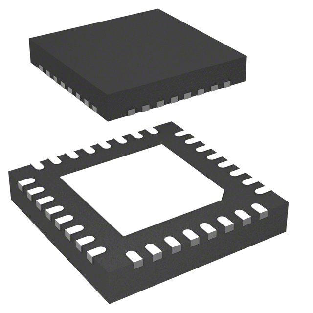
- Part No.:
- TDA8035HN/C1,151
- Manufacturer:
- NXP Semiconductors
- Category:
- Specialized
- Package:
- 32-VFQFN Exposed Pad
- Datasheet:
-
 TDA8035HN/C1,151.pdf
- Description:
- IC INTFACE SPECIALIZED 32HVQFN
- Quantity:
- Payment:

- Shipping:

Inventory:344
Please send an inquiry. Send us your inquiry, and we will respond immediately.
Product details
Overview
TDA8035HN/C1,151 from NXP Semiconductors is a highly integrated, low-power smart card interface IC designed for ISO 7816-compliant contact reader systems. It delivers regulated 5 V / 3 V / 1.8 V card supply (VCC), supports up to 20 MHz card clock generation, provides thermal/short-circuit protection on all card contacts, and achieves deep shutdown current as low as 0.1 µA - enabling power-efficient banking and pay-TV readers.
For engineers reviewing the TDA8035HN/C1,151 datasheet, TDA8035HN/C1,151 pinout, TDA8035HN/C1,151 application, or TDA8035HN/C1,151 equivalent, this page details verified electrical behavior, HVQFN32 package mapping, ISO 7816 fault-handling sequences, and real-world integration constraints including DC-DC converter capacitor ESR limits and synchronous CLKDIV frequency switching.
Technical Context
The TDA8035HN/C1,151 implements a dual-domain architecture: VDDP (2.7–5.5 V) powers the DC-DC converter and internal regulator (VREG = 1.8 V), while VDD(INTF) (1.6–3.6 V) supplies the host interface logic. Its clock circuitry auto-detects external XTAL1 input or crystal oscillator mode and supports synchronous fXTAL, fXTAL/2, fXTAL/4, or fXTAL/8 output via CLKDIV1/CLKDIV2 control.
Three protected bidirectional I/O lines (I/O, AUX1, AUX2) operate with 10 kΩ pull-ups referenced to VCC, while I/OUC, AUX1UC, AUX2UC are referenced to VDD(INTF); anti-latch arbitration ensures master/slave handshaking at ≤1.5 MHz. Fault detection triggers emergency deactivation on VCC short-circuit, card removal, VDDP/VREG/VDD(INTF) undervoltage, or overheating - signaled via OFFN.
Key Specifications
| Parameter | Value and Actual Design Meaning |
|---|---|
| VCC Output | 5 V ±5 %, 3 V ±5 %, or 1.8 V ±5 %; delivered via integrated DC-DC converter with overload detection at ~125 mA |
| Deep Shutdown Current | 0.1 µA typical; enables ultra-low-power standby in battery-powered card readers |
| Card Clock Frequency | Up to 20 MHz; selectable synchronously via CLKDIV1/CLKDIV2 (fXTAL, /2, /4, /8) |
| I/O Line Max Frequency | 1.5 MHz; supported on three half-duplex buffered lines (I/O, AUX1, AUX2) with active pull-up |
| ESD Protection | >8 kV HBM on card-side pins (I/O, RST, VCC, AUX1, CLK, AUX2, PRESN) |
| Operating Ambient Temp | −25 °C to +85 °C; validated for industrial and payment terminal environments |
| Package | HVQFN32 (SOT617-7); 5 × 5 × 0.85 mm body with thermal pad for 55 K/W junction-to-ambient dissipation |
Pinout & Package
HVQFN32 package (SOT617-7) with 32 terminals, 5 × 5 × 0.85 mm body, exposed thermal pad, and leadless construction optimized for thermal performance in compact card reader PCBs.
| Pin/Terminal | Circuit Role | Design Meaning |
|---|---|---|
| VCC (Pin 22) | Card supply output | Regulated 5 V / 3 V / 1.8 V output for ISO 7816 C1 contact; requires 2 × 220 nF low-ESR ceramic decoupling |
| RST (Pin 23) | Card reset output | Active-HIGH open-drain output to C2 contact; synchronized with activation/deactivation sequences |
| CLK (Pin 24) | Card clock output | Output to C3 contact; duty cycle 45–55 %; frequency set by CLKDIV1/CLKDIV2 and XTAL source |
| I/O (Pin 28) | Card data I/O | Half-duplex bidirectional line to C7 contact; 10 kΩ pull-up to VCC; max 15 mA current limit |
| PRESN (Pin 30) | Card presence input | Active-LOW input from mechanical switch; includes 4.05 ms hardware debounce |
| OFFN (Pin 10) | Fault interrupt output | Active-LOW NMOS open-drain interrupt to host; signals short-circuit, card removal, or supply fault |
| VDDP (Pin 18) | Main power supply | 2.7–5.5 V input powering DC-DC converter, VREG, and internal logic; monitored by voltage supervisor |
| VDD(INTF) (Pin 4) | Interface supply | 1.6–3.6 V supply for host-side logic (CS, CMDVCCN, RSTIN, CLKDIVx); PORADJ adjusts its threshold |
Key Features
| Feature | Design Value |
|---|---|
| Triple-voltage card supply generation | Single IC generates 5 V, 3 V, or 1.8 V VCC from 2.7–5.5 V VDDP using configurable DC-DC topology (doubler/tripler/follower) |
| Synchronous clock division | CLKDIV1/CLKDIV2 enable glitch-free, synchronous transitions between fXTAL, /2, /4, /8 without pulse distortion |
| Hardware-accelerated fault response | Automatic emergency deactivation within microseconds of VCC short-circuit or card removal - no host firmware intervention required |
| ISO 7816-compliant protection | Thermal shutdown, short-circuit limiting, and >8 kV HBM ESD protection on all card contacts (C1–C8) |
| Low-power multi-mode operation | Deep shutdown (0.1 µA), shutdown (300–500 µA), and active modes (5–220 mA) controlled via CMDVCCN, EN_5V/3VN, EN_1.8VN |
Applications
| Pay TV Conditional Access | EMV Banking Terminals |
|---|---|
|
Use Scenario: Secure decryption of encrypted video streams in set-top boxes using embedded SIM cards. IC Role / Device Role / Timing Role: Smart card interface IC managing VCC regulation, CLK timing, RST sequencing, and fault-safe deactivation during channel changes. Use Value: Enables <100 µs deactivation on card removal to prevent unauthorized key extraction; supports 20 MHz CLK for high-throughput DES/AES operations. |
Use Scenario: Chip-and-PIN transaction processing in point-of-sale terminals with EMV Level 1 compliance. IC Role / Device Role / Timing Role: ISO 7816 reader controller handling card activation, secure clock delivery, and real-time short-circuit detection during PIN entry. Use Value: Delivers 3 V ±5 % VCC with <300 mV ripple (20 kHz–200 MHz) to meet EMV 4.3 C2 version requirements for stable cryptographic execution. |
| Government ID Readers | Secure Access Control Systems |
|
Use Scenario: Biometric authentication and e-passport verification in border control kiosks. IC Role / Device Role / Timing Role: High-integrity card interface ensuring tamper-resistant power sequencing and ESD-hardened I/O for frequent card insertion cycles. Use Value: Built-in 4.05 ms PRESN debounce eliminates false card-present signals from mechanical switch bounce in high-traffic environments. |
Use Scenario: Physical access credential validation in enterprise door controllers with battery backup. IC Role / Device Role / Timing Role: Low-power smart card interface maintaining secure communication during mains failure using deep shutdown mode. Use Value: 0.1 µA deep shutdown current extends battery life to >5 years in always-on access readers with infrequent card use. |
Equivalent & Alternatives
The following parts are listed as comparable options for similar smart card interface applications.
| Alternative Part | Technical Difference | Application Difference | Selection Advice |
|---|---|---|---|
| TDA8034HN/C1 | Predecessor IC; lacks 1.8 V VCC support and enhanced ESD (>8 kV vs. 6 kV); identical HVQFN32 pinout and SW compatibility | Not certified for EMV 4.3 C2; limited to legacy 5 V/3 V-only card systems | Select when upgrading existing TDA8024 designs with minimal change and no 1.8 V requirement |
| SLB9670 | Trusted Platform Module (TPM) with integrated secure processor; no native ISO 7816 reader functionality - requires external reader IC | Designed for PC/platform root-of-trust, not standalone card readers | Choose only when system-level security certification (e.g., Common Criteria EAL4+) is mandatory and reader function is delegated |
Compared with TDA8034HN/C1, the TDA8035HN/C1,151 adds 1.8 V support and higher ESD robustness for modern low-voltage cards, while SLB9670 serves a fundamentally different security domain and cannot replace the TDA8035HN/C1,151 in direct smart card interfacing roles.
Availability
TDA8035HN/C1,151 is available at Aetrix Electronics and suitable for Pay TV conditional access modules, EMV banking terminals, and government ID readers requiring stable component supply, long lifecycle support, and full traceability.
Supply support for TDA8035HN/C1,151 includes scheduled delivery planning, volume procurement assistance, BOM continuity management, traceable sourcing, and lifecycle availability coordination for OEM customers, industrial embedded developers, connected-device designers, and electronics production programs.
Manufacturer
NXP Semiconductors is a global semiconductor leader specializing in secure connectivity solutions for automotive, industrial, and identification markets, with core expertise in smart card, NFC, and trusted execution technologies.
The TDA8035HN/C1,151 belongs to NXP's contact smart card reader IC product line, engineered specifically for cost-sensitive, low-power, and high-security ISO 7816 reader applications in payment, identity, and access control systems.
FAQ
What is the maximum allowable ESR for the 2 × 220 nF VCC decoupling capacitors in TDA8035HN/C1,151?
The TDA8035HN/C1,151 datasheet specifies that the two 220 nF ceramic capacitors on VCC must have ESR < 100 mΩ at 100 kHz. This low-ESR requirement ensures stable regulation under dynamic load conditions and prevents overshoot during activation. Exceeding this ESR may cause VCC ripple >300 mV (20 kHz–200 MHz), violating EMV 4.3 C2 compliance and risking card communication errors. Always verify capacitor datasheets for ESR curves across frequency.
Does TDA8035HN/C1,151 support automatic clock source selection between crystal and external clock?
Yes, the TDA8035HN/C1,151 automatically detects whether an external clock is applied to XTAL1 or if a crystal is connected across XTAL1/XTAL2. This detection occurs on each CMDVCCN falling edge, eliminating need for configuration pins. When external clock is present before CMDVCCN falls, the crystal oscillator remains stopped; otherwise, it starts. The TDA8035HN/C1,151 guarantees correct startup timing and avoids clock glitches during mode transition.
How does the TDA8035HN/C1,151 handle card removal during an active session?
During an active session (CMDVCCN = LOW), the TDA8035HN/C1,151 monitors PRESN and triggers immediate emergency deactivation upon first true-to-false transition - pulling RST LOW, stopping CLK, disabling I/O lines, and ramping VCC to zero within 250 µs. OFFN goes LOW to alert the host. After full deactivation, the host must reassert CMDVCCN HIGH and read OFFN to distinguish card removal from hardware fault based on OFFN reassertion.
What are the DC-DC converter capacitor requirements for TDA8035HN/C1,151 when generating 1.8 V VCC from 3.3 V VDDP?
For 1.8 V VCC generation from 3.3 V VDDP, the TDA8035HN/C1,151 operates in voltage doubler mode. It requires 330 nF capacitors on SAM–SAP and SBM–SBP (ESR < 100 mΩ at 100 kHz), plus a 1 µF decoupling capacitor on VUP–GNDP (same ESR spec). Using 100 nF instead of 330 nF is only valid when VDDP = 5 V - incorrect selection risks VCC instability and failed card activation sequences.
Is TDA8035HN/C1,151 pin-compatible with TDA8024, and what software changes are needed?
Yes, the TDA8035HN/C1,151 is software-compatible with TDA8024 and TDA8034 - same register map, command protocol, and activation/deactivation timing. No firmware changes are required for migration. However, TDA8035HN/C1,151 adds EN_1.8VN pin support for 1.8 V cards; leaving this pin unconnected defaults to 5 V/3 V mode, preserving full backward compatibility in legacy systems.
TDA8035HN/C1,151 Specifications
- Product attributes
- Attribute value
- Manufacturer:
- NXP Semiconductors
- Series:
- -
- Package/Case:
- 32-VFQFN Exposed Pad
- Packaging:
- Tray
- Product Status:
- Active
- Applications:
- -
- Interface:
- Analog
- Voltage - Supply:
- 1.8V, 3V, 5V
- Supplier Device Package:
- 32-HVQFN (5x5)
- Grade:
- -
- Qualification:
- -
- Mounting Type:
- Surface Mount
TDA8035HN/C1,151 FAQ
1.How can I place an order for TDA8035HN/C1,151 through Aetrix?
Please submit a Request for Quotation (RFQ) for TDA8035HN/C1,151 on Aetrix. Our sales agent will provide a competitive quotation and guide you through the order confirmation once you accept the terms.
2.Are the price and stock information for TDA8035HN/C1,151 reliable?
The price and inventory of TDA8035HN/C1,151 are updated periodically and may fluctuate due to market conditions. Stock and pricing data are typically refreshed every 24 hours. Quotation validity for TDA8035HN/C1,151 is usually 5 days.
3.What payment methods are accepted for TDA8035HN/C1,151?
We accept Wire Transfer, PayPal, Credit Card, Western Union, MoneyGram, and Escrow for TDA8035HN/C1,151 transactions.
Note: Certain payment methods may incur a processing fee.
4.How is shipping managed for TDA8035HN/C1,151?
TDA8035HN/C1,151 orders can be shipped via leading logistics carriers, including DHL, UPS, FedEx, TNT, or Registered Mail.
Once your TDA8035HN/C1,151 order is processed, you will receive an email with the shipment details and tracking number.
Note: Tracking information may take up to 24 hours to appear. Express delivery typically takes 3–5 business days.
5.How can I obtain technical support or documentation for TDA8035HN/C1,151?
For technical support, including TDA8035HN/C1,151 datasheets, pinout diagrams, or application guidance, please contact our engineering support team. They can provide detailed documentation and assistance for your TDA8035HN/C1,151 requirements.
6.How does Aetrix verify that TDA8035HN/C1,151 is sourced from the original manufacturer or authorized distributors?
All TDA8035HN/C1,151 products on Aetrix are procured from qualified distributors and authorized channels. Our dedicated quality assurance team conducts strict verification, including traceability checks and, if necessary, third-party testing. This ensures that TDA8035HN/C1,151 meets industry standards.
7.What is the process for return or replacement of TDA8035HN/C1,151?
All TDA8035HN/C1,151 units undergo pre-shipment inspection (PSI). If there is an issue with TDA8035HN/C1,151, returns or replacements are accepted under the following conditions:
1.Quantity discrepancies, incorrect items, or visible external defects (such as breakage or corrosion), acknowledged by Aetrix.
2.The issue is reported within 90 days of delivery.
3.The TDA8035HN/C1,151 part is unused and in its original packaging.
Return procedure for TDA8035HN/C1,151:
1.Submit a request within 90 days.
2.Obtain a Return Material Authorization (RMA) from Aetrix.
TDA8035HN/C1,151 Tags

-
NVT4857UKAZ
NXP Semiconductors

-
TCA8418RTWR
Texas Instruments

-
PCA9546APWR
Texas Instruments

-
MD0100N8-G
Microchip Technology

-
PCA9548APW,118
NXP Semiconductors

-
PCA9540BDP,118
NXP Semiconductors

-
PCA9548APWR
Texas Instruments

-
PCA9546APW,118
NXP Semiconductors

-
PTN3360DBS,518
NXP Semiconductors

-
PCA9546ABS,118
NXP Semiconductors

-
PCA9518PWR
Texas Instruments

-
PCA9545APW,118
NXP Semiconductors
Tech Hub

A practical engineering guide to 3.3V and 5V logic compatibility, input thresholds, resistor dividers, translator ICs, MOSFET level shifting, I2C pull-ups, timing limits and power-sequencing risks.

The 74HC595 uses push-pull logic outputs, while the TPIC6B595 uses 50 V open-drain DMOS sinks for higher-power loads. This guide compares timing, current limits, 3.3 V interfacing, load wiring, thermal…

The 74HC595 converts serial data into eight stable parallel outputs. This guide covers pin functions, shift and storage timing, OE and MR behavior, drive-current limits, cascading, voltage compatibilit…

A technical comparison of level-sensitive latches and edge-triggered flip-flops, covering timing windows, setup and hold limits, master–slave operation, time borrowing, race-through, HDL inference and…

A D latch stores one bit while Enable controls when data can pass. This reference covers gate-level operation, truth tables, transparency, setup and hold timing, LE versus OE, common ICs and practical …

An SR latch stores one bit through cross-coupled feedback. This engineering reference covers NOR and NAND implementations, truth tables, forbidden-state recovery, gated operation, switch debouncing, fa…

Latch circuits retain one bit through feedback. This technical reference covers SR and D latches, truth tables, transparency, timing limits, latch-versus-flip-flop behavior, applications and common log…

An engineering guide to LED driver operation, constant-current and constant-voltage outputs, linear and switching topologies, dimming, IC selection, calculations, replacement compatibility, and fault c…

Operational amplifier guide covering op amp basics, feedback, ideal vs real op amps, common configurations, buffer circuits, offset, bias current, gain-bandwidth, slew rate, rail-to-rail limits and sel…

Jumper cables guide covering safe connection order, red and black clamp placement, final ground connection, cable gauge, length, clamp quality, copper vs CCA cables, jump starter comparison and battery…


