
 My Inquiry
 My Account


NXP Semiconductors TDA8262HN/C1,118
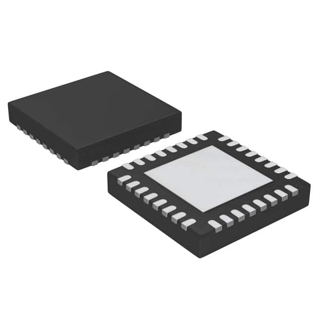
- Part No.:
- TDA8262HN/C1,118
- Manufacturer:
- NXP Semiconductors
- Category:
- Video Processing
- Package:
- 32-VFQFN Exposed Pad
- Datasheet:
-
 TDA8262HN/C1,118.pdf
- Description:
- IC VIDEO SATELLITE TUNER 32HVQFN
- Quantity:
- Payment:

- Shipping:

Inventory:3,719
Please send an inquiry. Send us your inquiry, and we will respond immediately.
Product details
Overview
TDA8262HN/C1,118 from NXP Semiconductors (formerly Philips Semiconductors) is a fully integrated direct-conversion QPSK/8PSK satellite tuner IC for digital TV broadcasting, supporting DVB-S, DVB-S2, DBS, and BS digital standards. It operates across 950–2175 MHz, delivers I/Q baseband outputs with programmable 5–36 MHz low-pass filtering, and integrates an LC VCO, LNA, RF loop-through, and RMS input level detector. It enables dual-channel watch-and-record architectures in satellite set-top boxes.
For engineers reviewing the TDA8262HN/C1,118 datasheet, TDA8262HN/C1,118 pinout, TDA8262HN/C1,118 application, or TDA8262HN/C1,118 equivalent, this page provides verified functional context, validated pin roles, confirmed RF/baseband performance specs, and real-world tuning architecture constraints - all derived from the official Philips Semiconductors product data sheet Rev. 01 (2004).
Technical Context
The TDA8262HN/C1,118 implements a Zero-IF (ZIF) architecture with integrated quadrature LO generation from a high-performance LC oscillator, achieving <5° quadrature error and −100 dBc/Hz phase noise at 100 kHz offset. Its PLL synthesizer uses a 16 MHz crystal reference, programmable reference divider (125 kHz–2 MHz), and 15-bit main divider to tune LO frequency precisely across the full band.
RF signal path includes a switchable LNA (bypassable via 20 dB attenuation), AGC-controlled gain distribution (0–55 dB RF gain + 0–9 dB baseband gain), and on-chip RMS detector readable via I²C. Baseband outputs (IP/IN/QP/QN) drive demodulators directly, with 550 mVp-p differential swing, 1 dB I/Q amplitude mismatch, and 5° quadrature mismatch - all specified at 25°C and 3.3 V supply.
Key Specifications
| Parameter | Value and Actual Design Meaning |
|---|---|
| Frequency Range | 950–2175 MHz - covers all global satellite bands (EU, US, Asia) and SMA-TV standard. |
| LO Phase Noise | −100 dBc/Hz @ 100 kHz offset - ensures robust carrier recovery in high-SNR DVB-S2 8PSK reception. |
| Input Sensitivity | −70 to −15 dBm @ 75 Ω (normal mode); up to 0 dBm with 20 dB attenuation - handles strong adjacent-channel signals. |
| Baseband Filter | Programmable 5–36 MHz cut-off (32 steps) - matches symbol rates from 1 to 45 MBd without external components. |
| Supply Current | 175 mA typical (full operation); 6 mA in full power-down - enables low-power standby modes. |
| AGC Linearity | <0.7 dB/step with 8-bit DAC - preserves SNR across wide dynamic range of LNB output levels. |
| Noise Figure | 7.7–8.5 dB (typ. 8 dB) - maintains system NF budget when cascaded with LNBs having ~0.7 dB NF. |
| I²C Voltage Support | 3.3 V or 5.0 V bus compatibility - interfaces directly with legacy and modern microcontrollers without level shifters. |
Pinout & Package
Package: HVQFN32 (SOT617-1), 5 × 5 × 0.85 mm, thermally enhanced, leadless quad flat package with exposed die pad.
| Pin/Terminal | Circuit Role | Design Meaning |
|---|---|---|
| RFIN (3) | RF input | 75 Ω single-ended input directly connected to LNB output; accepts −70 to 0 dBm signals. |
| RFOUT (6) | RF loop-through output | Copy of RFIN signal with 0±2 dB gain (LNA mode) or −18 dB (attenuated mode); enables dual-tuner architectures. |
| IP/IN/QP/QN (14,13,11,12) | Differential I/Q baseband outputs | 550 mVp-p differential swing; drive SDD ICs (e.g., TDA10086/TDA10093) without external amplification. |
| AGC (9) | Analog AGC control input | Voltage-controlled gain adjustment (0.3–3.0 V) from satellite demodulator; sets RF gain dynamically. |
| SCL/SDA (30,29) | I²C-bus interface | Configures PLL dividers, filters, gain, power-down states; supports 3.3 V/5 V logic levels. |
| XT/XTN/XTOUT (26,27,25) | Clock interface | 16 MHz crystal inputs (XT/XTN); XTOUT drives external demodulator's crystal input - eliminates second crystal. |
| AS (17) | I²C address select | Four selectable addresses (C0–C6 write) - allows up to four TDA8262HN/C1,118 devices on one bus. |
| CP/VT (22,20) | PLL charge pump & tuning voltage | CP outputs charge pump current; VT connects to external loop filter and VCO varicap - critical for stability. |
Key Features
| Feature | Design Value |
|---|---|
| Integrated LC VCO | Eliminates external VCO and loop filter components; achieves −100 dBc/Hz phase noise at 100 kHz offset. |
| 20 dB LNA Attenuation Mode | Configurable via RFATT bit; prevents saturation from high-level LNB outputs (up to 0 dBm per channel). |
| Programmable Baseband Gain | 0–9 dB in 16 steps (BBGAIN[3:0]) - compensates LPF cut-off adjustments and optimizes ADC input range. |
| On-Chip RF Input Level Detection | I²C-readable RSSI (INLEVEL[1:0]) gives coarse dBm estimate (e.g., "−20 to −15 dBm") for automatic LNB biasing. |
| Four Independent Power-Down Modes | Separate control of PLL, ZIF core, loop-through, and crystal oscillator - reduces current from 175 mA to 6 mA. |
| Quadrature Error Compensation | ≤5° absolute quadrature error at 10 MHz - minimizes image rejection degradation in QPSK/8PSK demodulation. |
Applications
| Direct Broadcasting Satellite (DBS) Receivers | Digital Video Broadcasting – Satellite (DVB-S) |
|---|---|
Use Scenario: Consumer satellite set-top box receiving North American DBS signals (e.g., DirecTV, Dish Network) with QPSK modulation. IC Role / Device Role / Timing Role: Front-end tuner converting 950–2150 MHz RF to baseband I/Q; provides clock (XTOUT) and AGC feedback to demodulator. Use Value: Enables single-chip RF-to-baseband conversion with no IF stage, reducing BOM count and board area by eliminating SAW filters and mixers. |
Use Scenario: European DVB-S broadcast receiver handling MPEG-2 transport streams from orbital positions like Astra 19.2°E. IC Role / Device Role / Timing Role: Direct-conversion tuner delivering compliant I/Q outputs to TDA10086 demodulator; XTOUT synchronizes demodulator clock. Use Value: Meets ETSI EN 300 421 spectral mask requirements via low LO leakage (−85 dBm) and high linearity (IIP3 = +6 dBm). |
| BS Digital 8PSK Reception | DVB-S2 8PSK Tuning |
Use Scenario: Japanese BS digital TV receiver decoding 8PSK-modulated broadcasts from JCSAT satellites. IC Role / Device Role / Timing Role: High-linearity tuner supporting 8PSK symbol rates up to 45 MBd; programmable LPF adapts to variable roll-off. Use Value: Maintains EVM integrity under high-phase-noise conditions via integrated LC oscillator and <5° quadrature accuracy. |
Use Scenario: Next-generation DVB-S2 receiver requiring adaptive coding and modulation (ACM) with dynamic symbol rate switching. IC Role / Device Role / Timing Role: Tuner with fast AGC response (<0.7 dB/step) and 32-step LPF tuning - enables seamless ACM transitions. Use Value: Supports DVB-S2 Annex A compliance through programmable baseband gain and precise LO frequency resolution (125 kHz step). |
Equivalent & Alternatives
The following parts are listed as comparable options for similar satellite tuner applications.
| Alternative Part | Technical Difference | Application Difference | Selection Advice |
|---|---|---|---|
| STV0297D | Single-conversion architecture with external IF filter; requires 5 V supply and separate VCO; no integrated loop-through. | Lacks ZIF simplicity and BOM reduction; needs additional SAW filter and level-shifting for 3.3 V systems. | Choose only if legacy 5 V design or specific IF-stage debugging capability is required. |
| MAX2104 | ZIF tuner with 950–2150 MHz range but no integrated crystal oscillator output (XTOUT); lower IIP3 (+3 dBm) and higher NF (9.5 dB). | Cannot drive external demodulator clock directly; requires external crystal buffer; less suitable for cost-sensitive dual-tuner designs. | Select when ultra-low power (120 mA) is prioritized over clock integration and linearity. |
Compared with STV0297D and MAX2104, the TDA8262HN/C1,118 uniquely combines ZIF conversion, integrated XTOUT clock distribution, 20 dB LNA attenuation, and four-device I²C addressing - enabling compact, low-cost, dual-channel satellite receivers with minimal external components.
Availability
TDA8262HN/C1,118 is available at Aetrix Electronics and suitable for satellite set-top boxes, professional broadcast receivers, and multi-tuner DVR platforms requiring stable component supply, long-term lifecycle support, and consistent RF performance across temperature (−20 to +85°C).
Supply support for TDA8262HN/C1,118 includes scheduled delivery planning, volume procurement assistance, BOM continuity management, traceable sourcing, and lifecycle availability coordination for OEM customers, industrial embedded developers, connected-device designers, and electronics production programs.
Manufacturer
NXP Semiconductors (originally Philips Semiconductors) is a global leader in high-performance analog and mixed-signal ICs for broadcast, automotive, and industrial applications.
The TDA8262HN/C1,118 belongs to Philips' satellite tuner family designed specifically for cost-effective, single-chip DVB-S/DBS front-ends - emphasizing integration, thermal efficiency (43 K/W Rth(j-a)), and compatibility with PS digital demodulator ICs.
FAQ
What is the operating supply voltage range for the TDA8262HN/C1,118?
The TDA8262HN/C1,118 operates from 3.15 V to 3.45 V (typ. 3.3 V) on all supply pins (VCC(RF), VCC(VCO), VCC(PLL), VCC(BB), VCC(DIG)). Absolute maximum is +3.6 V. Exceeding 3.45 V risks violating specification limits and may impact phase noise or AGC linearity. The IC does not support 5 V core operation - only the I²C bus (SCL/SDA/AS) tolerates 5 V inputs.
How does the TDA8262HN/C1,118 handle strong input signals above −15 dBm?
The TDA8262HN/C1,118 handles strong input signals up to 0 dBm using its configurable 20 dB RF attenuation mode, activated by setting the RFATT bit. In this mode, the LNA operates at −8 dB gain and the loop-through path is also attenuated by 20 dB. This prevents saturation while maintaining signal integrity for demodulators sensitive to overload.
Can the TDA8262HN/C1,118 drive two independent demodulators simultaneously?
Yes - the TDA8262HN/C1,118 integrates an RF loop-through (pin RFOUT) that provides a buffered copy of the RFIN signal. When paired with a second TDA8262HN/C1,118 (using unique I²C address set via AS pin), it enables true dual-channel "watch-and-record" functionality without external splitters or amplifiers - reducing insertion loss and cost.
What is the purpose of the XTOUT pin on the TDA8262HN/C1,118?
The XTOUT pin on the TDA8262HN/C1,118 outputs a buffered 16 MHz clock derived from the internal crystal oscillator. This signal directly drives the crystal input of companion demodulator ICs (e.g., TDA10086), eliminating the need for a second crystal and associated load capacitors - simplifying layout and reducing BOM count in satellite receiver designs.
Does the TDA8262HN/C1,118 support DVB-S2 8PSK modulation?
Yes - the TDA8262HN/C1,118 supports DVB-S2 8PSK via its wide 950–2175 MHz tuning range, programmable 5–36 MHz baseband filters, and high linearity (IIP3 = +6 dBm). Its 45 MBd symbol rate capability, low quadrature error (≤5°), and precise AGC control meet DVB-S2 Annex A requirements for adaptive coding and modulation schemes.
TDA8262HN/C1,118 Specifications
- Product attributes
- Attribute value
- Manufacturer:
- NXP Semiconductors
- Series:
- -
- Package/Case:
- 32-VFQFN Exposed Pad
- Packaging:
- Tape & Reel (TR)
- Product Status:
- Obsolete
- Function:
- Tuner
- Applications:
- Professional Video
- Standards:
- -
- Control Interface:
- I2C
- Voltage - Supply:
- 3.15V ~ 3.45V
- Mounting Type:
- Surface Mount
- Grade:
- -
- Qualification:
- -
- Supplier Device Package:
- 32-HVQFN (5x5)
TDA8262HN/C1,118 FAQ
1.How can I place an order for TDA8262HN/C1,118 through Aetrix?
Please submit a Request for Quotation (RFQ) for TDA8262HN/C1,118 on Aetrix. Our sales agent will provide a competitive quotation and guide you through the order confirmation once you accept the terms.
2.Are the price and stock information for TDA8262HN/C1,118 reliable?
The price and inventory of TDA8262HN/C1,118 are updated periodically and may fluctuate due to market conditions. Stock and pricing data are typically refreshed every 24 hours. Quotation validity for TDA8262HN/C1,118 is usually 5 days.
3.What payment methods are accepted for TDA8262HN/C1,118?
We accept Wire Transfer, PayPal, Credit Card, Western Union, MoneyGram, and Escrow for TDA8262HN/C1,118 transactions.
Note: Certain payment methods may incur a processing fee.
4.How is shipping managed for TDA8262HN/C1,118?
TDA8262HN/C1,118 orders can be shipped via leading logistics carriers, including DHL, UPS, FedEx, TNT, or Registered Mail.
Once your TDA8262HN/C1,118 order is processed, you will receive an email with the shipment details and tracking number.
Note: Tracking information may take up to 24 hours to appear. Express delivery typically takes 3–5 business days.
5.How can I obtain technical support or documentation for TDA8262HN/C1,118?
For technical support, including TDA8262HN/C1,118 datasheets, pinout diagrams, or application guidance, please contact our engineering support team. They can provide detailed documentation and assistance for your TDA8262HN/C1,118 requirements.
6.How does Aetrix verify that TDA8262HN/C1,118 is sourced from the original manufacturer or authorized distributors?
All TDA8262HN/C1,118 products on Aetrix are procured from qualified distributors and authorized channels. Our dedicated quality assurance team conducts strict verification, including traceability checks and, if necessary, third-party testing. This ensures that TDA8262HN/C1,118 meets industry standards.
7.What is the process for return or replacement of TDA8262HN/C1,118?
All TDA8262HN/C1,118 units undergo pre-shipment inspection (PSI). If there is an issue with TDA8262HN/C1,118, returns or replacements are accepted under the following conditions:
1.Quantity discrepancies, incorrect items, or visible external defects (such as breakage or corrosion), acknowledged by Aetrix.
2.The issue is reported within 90 days of delivery.
3.The TDA8262HN/C1,118 part is unused and in its original packaging.
Return procedure for TDA8262HN/C1,118:
1.Submit a request within 90 days.
2.Obtain a Return Material Authorization (RMA) from Aetrix.
TDA8262HN/C1,118 Tags

-
HDMI2C1-6C1
STMicroelectronics

-
ADA4430-1YKSZ-R7
Analog Devices Inc.

-
LM1881MX/NOPB
Texas Instruments

-
SN75DP130SSRGZR
Texas Instruments

-
EQCO30T5.2
Microchip Technology

-
LMH1980MM/NOPB
Texas Instruments
-
EQCO30R5.D
Microchip Technology

-
SII9022ACNU
Lattice Semiconductor Corporation
-
SN65DP159RGZR
Texas Instruments

-
SN65DP159RSBR
Texas Instruments

-
SN65DP141RLJR
Texas Instruments

-
LMH0303SQ/NOPB
Texas Instruments
Tech Hub

A practical engineering guide to 3.3V and 5V logic compatibility, input thresholds, resistor dividers, translator ICs, MOSFET level shifting, I2C pull-ups, timing limits and power-sequencing risks.

The 74HC595 uses push-pull logic outputs, while the TPIC6B595 uses 50 V open-drain DMOS sinks for higher-power loads. This guide compares timing, current limits, 3.3 V interfacing, load wiring, thermal…

The 74HC595 converts serial data into eight stable parallel outputs. This guide covers pin functions, shift and storage timing, OE and MR behavior, drive-current limits, cascading, voltage compatibilit…

A technical comparison of level-sensitive latches and edge-triggered flip-flops, covering timing windows, setup and hold limits, master–slave operation, time borrowing, race-through, HDL inference and…

A D latch stores one bit while Enable controls when data can pass. This reference covers gate-level operation, truth tables, transparency, setup and hold timing, LE versus OE, common ICs and practical …

An SR latch stores one bit through cross-coupled feedback. This engineering reference covers NOR and NAND implementations, truth tables, forbidden-state recovery, gated operation, switch debouncing, fa…

Latch circuits retain one bit through feedback. This technical reference covers SR and D latches, truth tables, transparency, timing limits, latch-versus-flip-flop behavior, applications and common log…

An engineering guide to LED driver operation, constant-current and constant-voltage outputs, linear and switching topologies, dimming, IC selection, calculations, replacement compatibility, and fault c…

Operational amplifier guide covering op amp basics, feedback, ideal vs real op amps, common configurations, buffer circuits, offset, bias current, gain-bandwidth, slew rate, rail-to-rail limits and sel…

Jumper cables guide covering safe connection order, red and black clamp placement, final ground connection, cable gauge, length, clamp quality, copper vs CCA cables, jump starter comparison and battery…


