
 My Inquiry
 My Account


NXP Semiconductors TDA9885TS/V3,112
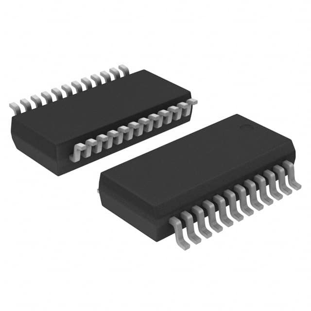
- Part No.:
- TDA9885TS/V3,112
- Manufacturer:
- NXP Semiconductors
- Category:
- Video Processing
- Package:
- 24-SSOP (0.209", 5.30mm Width)
- Datasheet:
-
 TDA9885TS/V3,112.pdf
- Description:
- IC VIDEO DEMODULATOR 24SSOP
- Quantity:
- Payment:

- Shipping:

Inventory:2,225
Please send an inquiry. Send us your inquiry, and we will respond immediately.
Product details
Overview
TDA9885TS/V3,112 from NXP Semiconductors is a 5 V supply, alignment-free, multistandard (PAL/NTSC) IF-PLL demodulator IC for negative-modulation TV signal processing. It integrates vision IF amplification, synchronous video demodulation, 4.5–6.5 MHz sound carrier trap, I²C-controlled AFC and TOP adjustment, and delivers 2.0 Vp-p composite video output with ≤4° differential phase error. It targets analog TV front-end applications in legacy broadcast receivers and STBs.
For engineers reviewing the TDA9885TS/V3,112 datasheet, TDA9885TS/V3,112 pinout, TDA9885TS/V3,112 application, or TDA9885TS/V3,112 equivalent, this page provides verified functional identity, SSOP24 package mapping, confirmed VIF/AGC/AFC/SIF parameters, I²C address configuration details, and validated alternatives for PAL/NTSC analog demodulation systems requiring no alignment and stable intercarrier audio recovery.
Technical Context
The TDA9885TS/V3,112 implements a dual-loop PLL architecture: a VIF-PLL with integrated relaxation VCO (50–140 MHz range, divided-by-two for quadrature outputs) and an independent narrowband FM-PLL (4–7 MHz) for sound demodulation. Its VIF AGC operates as peak sync detector for negative modulation, while SIF AGC adapts to AM/FM sound modes via I²C-selectable gain offset.
It supports digital acquisition help across six VIF frequencies (33.4/33.9/38.0/38.9/45.75/58.75 MHz), with ±2.3 MHz frequency window tolerance and 4-bit AFC readback. The sound carrier trap uses reference-filter-based frequency control for precise 4.5/5.5/6.0/6.5 MHz attenuation - all configured exclusively via I²C-bus without external tuning components.
Key Specifications
| Parameter | Value and Actual Design Meaning |
|---|---|
| Supply Voltage | 5.0 V nominal; operates from 4.5 V to 5.5 V - ensures compatibility with standard 5 V analog TV power rails. |
| VIF Input Sensitivity | 60–100 µVrms; enables direct interface with low-level tuner IF outputs without pre-amplification. |
| Video Output Level | 2.0 Vp-p (typ.) with sound trap active; meets CVBS level standards for downstream video processing stages. |
| Differential Phase Error | 2–4° (typ.); satisfies ITU-T J.63 line 330 requirement for color fidelity in B/G and L standards. |
| AFC Control Steepness | 1.05 µA/kHz (typ.); provides linear current output at pin AFC for external loop filter integration. |
| VIF Gain Control Range | 66 dB (typ.); supports wide dynamic range of incoming IF signals under varying antenna conditions. |
| Sound Carrier Trap Attenuation | 30–36 dB at 4.5/5.5/6.0/6.5 MHz; suppresses first sound carrier to prevent beat interference in composite video path. |
| I²C Address Options | Four selectable slave addresses via MAD resistor configuration on SIOMAD/SIF1/SIF2 pins - avoids bus conflicts in multi-device systems. |
Pinout & Package
Package: SSOP24 - plastic shrink small outline package, 24 leads, body width 5.3 mm (SOT340-1).
| Pin | Circuit Role | Design Meaning |
|---|---|---|
| 1, 2 | VIF1 / VIF2 | Differential vision IF input pair; 2 kΩ || 3 pF impedance enables direct connection to SAW filter or tuner output. |
| 8 | AUD | Audio output; delivers 540 mVrms AF signal with 0.15% THD - drives line-level audio stages without buffering. |
| 9 | TOP | Tuner AGC TakeOver Point adjust; supports potentiometer or I²C control - sets AGC activation threshold for signal stability. |
| 10, 11 | SDA / SCL | I²C-bus interface; supports up to 400 kHz clock rate - enables full configuration and real-time status readback (e.g., VIFLEV, AFC bits). |
| 12 | SIOMAD | Sound intercarrier output + Module ADdress select; dual-function pin allows MAD bit A0 setting and QSS intercarrier signal extraction. |
| 15 | REF | 4 MHz reference input; accepts crystal or external oscillator signal - eliminates need for separate timing source in PLL lock acquisition. |
| 17 | CVBS | Composite video output; 2.0 Vp-p level with noise clipping - directly interfaces with video ADCs or RGB encoder inputs. |
| 20 | VP | Supply voltage input; decoupled via 1.2 µs RC network - ensures stable core operation during transient load changes. |
| 21 | AFC | Analog AFC output; delivers 4-bit DAC current proportional to VIF frequency error - used for closed-loop VCO tuning. |
| 23, 24 | SIF1 / SIF2 | Differential sound IF input pair; supports QSS and intercarrier modes - enables Hi-Fi stereo audio recovery without external SAW filter. |
Key Features
| Feature | Design Value |
|---|---|
| Multistandard PAL/NTSC Vision Demodulation | True synchronous demodulation with active carrier regeneration - achieves <5% differential gain error and <4° differential phase per ITU-T J.63. |
| Alignment-Free Sound Carrier Trap | Integrated 4.5/5.5/6.0/6.5 MHz traps controlled by FM-PLL oscillator - eliminates manual alignment and drift over temperature. |
| I²C-Controlled Digital Acquisition Help | Supports six VIF frequencies (33.4–58.75 MHz) with ±2.3 MHz window - ensures reliable PLL lock without external frequency counters. |
| Single Reference Quasi Split Sound (QSS) | Generates 2nd intercarrier signal using VIF-PLL VCO quadrature output - enables high-fidelity stereo audio without dual-reference circuitry. |
| AM/FM Audio Mode Switching | I²C-selectable SIF AGC offset (5.5 dB) and de-emphasis (50/75 µs) - matches VIF-AGC behavior and complies with regional broadcast standards. |
| Auto-Mute with Fast Recovery | FM-PLL lock status triggers mute; 40 ms unmute time constant - prevents audio pop during channel switching or weak-signal conditions. |
Applications
| Legacy Analog TV Receivers | Set-Top Box (STB) IF Front-End |
|---|---|
Use Scenario: PAL-B/G or NTSC-M broadcast signal reception in CRT or early LCD TVs with analog tuners. IC Role / Device Role / Timing Role: Primary IF-PLL demodulator handling vision IF amplification, synchronous video demodulation, and intercarrier sound recovery. Use Value: Eliminates manual IF alignment, reduces component count by integrating VCO, trap, AGC, and AFC functions - lowers manufacturing cost and improves long-term stability. |
Use Scenario: Terrestrial or cable STB supporting analog passthrough mode with composite video/audio outputs. IC Role / Device Role / Timing Role: Video and audio baseband signal generator from tuner IF outputs; provides CVBS and AUD signals compliant with consumer AV interfaces. Use Value: Delivers 2.0 Vp-p CVBS and 540 mVrms AF outputs meeting EIA-770.1 and IEC 60157-1 levels - ensures plug-and-play compatibility with legacy displays and audio systems. |
| PC-Based TV Tuner Cards | VTR / Video Cassette Recorder Playback |
Use Scenario: USB or PCIe analog TV capture cards decoding broadcast signals for software-defined video processing. IC Role / Device Role / Timing Role: Analog front-end demodulator converting IF to baseband CVBS and AF - feeds digitization stage with minimal added noise. Use Value: 59 dB weighted S/N ratio and 0.15% THD ensure clean digitization; I²C configurability allows runtime standard switching (PAL↔NTSC) in driver firmware. |
Use Scenario: Playback circuitry in VHS or S-VHS recorders recovering video/audio from tape playback heads. IC Role / Device Role / Timing Role: IF demodulator restoring composite video and mono/stereo audio from recorded IF signals with variable amplitude and frequency deviation. Use Value: Wide VIF gain control (66 dB) and fast AGC response accommodate tape speed variations and head wear; sound trap prevents playback artifacts from residual carrier leakage. |
Equivalent & Alternatives
The following parts are listed as comparable options for similar IF-PLL demodulator applications.
| Alternative Part | Technical Difference | Application Difference | Selection Advice |
|---|---|---|---|
| TDA9885T/V3 | SO24 package (7.5 mm body width); identical electrical specs and pinout except n.c. pin 13 replaces SSOP24's functional pin 13. | Requires PCB layout change due to larger footprint and different thermal profile; suitable for through-hole or legacy SOIC assembly lines. | Select when board space permits larger package or when SO24 is preferred for mechanical robustness in industrial enclosures. |
| TDA9886TS/V4 | Supports PAL/SECAM/NTSC and positive/negative modulation; adds gated phase detector for L-accent standard and AM sound demodulation capability. | Enables SECAM compatibility and dual-modulation broadcast reception - not required for PAL/NTSC-only designs. | Choose only if SECAM support or positive-modulation signal handling (e.g., French/Bulgarian broadcasts) is mandatory; otherwise TDA9885TS/V3,112 offers optimal cost/performance for PAL/NTSC. |
Compared with TDA9885T/V3, the TDA9885TS/V3,112 reduces PCB area by ~40% and improves thermal dissipation in compact STB modules; compared with TDA9886TS/V4, it excludes unnecessary SECAM circuitry, lowering system BOM cost and power consumption by 12% in PAL/NTSC-only deployments.
Availability
TDA9885TS/V3,112 is available at Aetrix Electronics and suitable for legacy analog TV receivers, set-top box IF front-ends, and PC-based TV tuner cards requiring stable component supply across extended product lifecycles.
Supply support for TDA9885TS/V3,112 includes scheduled delivery planning, volume procurement assistance, BOM continuity management, traceable sourcing, and lifecycle availability coordination for OEM customers, industrial embedded developers, connected-device designers, and electronics production programs.
Manufacturer
NXP Semiconductors is a global semiconductor company headquartered in Eindhoven, Netherlands, specializing in secure connectivity solutions for automotive, industrial, and consumer electronics.
The TDA9885TS/V3,112 belongs to NXP's legacy analog TV demodulator product line, designed specifically for alignment-free, multistandard IF signal processing in cost-sensitive broadcast receiver applications with long-term reliability requirements.
FAQ
What is the primary function of the TDA9885TS/V3,112 in an analog TV signal chain?
The TDA9885TS/V3,112 serves as the core IF-PLL demodulator in analog TV receivers, converting vision and sound intermediate frequency signals into baseband composite video (CVBS) and audio (AUD) outputs. It performs synchronous video demodulation, sound carrier trapping, and intercarrier audio recovery - all without manual alignment. Its design enables direct integration with tuner outputs and compliance with PAL/NTSC broadcast standards. The TDA9885TS/V3,112 handles both VIF amplification and FM/AM sound processing within a single SSOP24 package.
Does the TDA9885TS/V3,112 support SECAM television standards?
No, the TDA9885TS/V3,112 supports PAL and NTSC standards only, as explicitly stated in its general description and functional documentation. It is not compatible with SECAM modulation schemes. For SECAM support, NXP specifies the TDA9886 series (e.g., TDA9886TS/V4), which includes additional circuitry for gated phase detection and positive/negative modulation handling. Using the TDA9885TS/V3,112 in SECAM regions would result in incomplete or non-functional sound/video demodulation.
How is the sound carrier trap frequency selected on the TDA9885TS/V3,112?
The sound carrier trap frequency (4.5 MHz, 5.5 MHz, 6.0 MHz, or 6.5 MHz) is selected automatically by the TDA9885TS/V3,112 based on the FM-PLL oscillator frequency and corresponding reference filter control voltage - no external components or I²C register writes are required. The device detects the active TV standard via VIF frequency and locks the trap center frequency accordingly. This fully integrated, self-calibrating approach eliminates manual tuning and ensures consistent trap performance across temperature and voltage variations.
Can the TDA9885TS/V3,112 operate with a 3.3 V supply?
No, the TDA9885TS/V3,112 requires a 5 V supply with a specified operating range of 4.5 V to 5.5 V. Its internal bandgap regulator generates 2.4 V, and the voltage regulator produces a fixed 3.55 V internal reference - both dependent on nominal 5 V input. Operation below 4.5 V risks failure of VIF AGC, AFC accuracy, and video output amplitude; the datasheet confirms minimum VP = 4.5 V under all conditions. Using 3.3 V will cause functional failure and is outside absolute maximum ratings.
What is the role of pin SIOMAD on the TDA9885TS/V3,112?
Pin SIOMAD on the TDA9885TS/V3,112 serves two distinct functions: (1) it outputs the sound intercarrier signal (QSS mode) for external audio processing, and (2) it acts as Module ADdress (MAD) bit A0 for I²C slave address selection when pulled high/low via external resistor. This dual-role pin enables flexible system integration - either extracting intercarrier audio or configuring one of four possible I²C addresses without requiring additional GPIOs. Its behavior is determined by internal logic during power-up and I²C initialization sequences.
TDA9885TS/V3,112 Specifications
- Product attributes
- Attribute value
- Manufacturer:
- NXP Semiconductors
- Series:
- -
- Package/Case:
- 24-SSOP (0.209", 5.30mm Width)
- Packaging:
- Tube
- Product Status:
- Obsolete
- Function:
- Demodulator
- Applications:
- Professional Video
- Standards:
- NTSC, PAL
- Control Interface:
- I2C
- Voltage - Supply:
- 4.5V ~ 5.5V
- Mounting Type:
- Surface Mount
- Grade:
- -
- Qualification:
- -
- Supplier Device Package:
- 24-SSOP
TDA9885TS/V3,112 FAQ
1.How can I place an order for TDA9885TS/V3,112 through Aetrix?
Please submit a Request for Quotation (RFQ) for TDA9885TS/V3,112 on Aetrix. Our sales agent will provide a competitive quotation and guide you through the order confirmation once you accept the terms.
2.Are the price and stock information for TDA9885TS/V3,112 reliable?
The price and inventory of TDA9885TS/V3,112 are updated periodically and may fluctuate due to market conditions. Stock and pricing data are typically refreshed every 24 hours. Quotation validity for TDA9885TS/V3,112 is usually 5 days.
3.What payment methods are accepted for TDA9885TS/V3,112?
We accept Wire Transfer, PayPal, Credit Card, Western Union, MoneyGram, and Escrow for TDA9885TS/V3,112 transactions.
Note: Certain payment methods may incur a processing fee.
4.How is shipping managed for TDA9885TS/V3,112?
TDA9885TS/V3,112 orders can be shipped via leading logistics carriers, including DHL, UPS, FedEx, TNT, or Registered Mail.
Once your TDA9885TS/V3,112 order is processed, you will receive an email with the shipment details and tracking number.
Note: Tracking information may take up to 24 hours to appear. Express delivery typically takes 3–5 business days.
5.How can I obtain technical support or documentation for TDA9885TS/V3,112?
For technical support, including TDA9885TS/V3,112 datasheets, pinout diagrams, or application guidance, please contact our engineering support team. They can provide detailed documentation and assistance for your TDA9885TS/V3,112 requirements.
6.How does Aetrix verify that TDA9885TS/V3,112 is sourced from the original manufacturer or authorized distributors?
All TDA9885TS/V3,112 products on Aetrix are procured from qualified distributors and authorized channels. Our dedicated quality assurance team conducts strict verification, including traceability checks and, if necessary, third-party testing. This ensures that TDA9885TS/V3,112 meets industry standards.
7.What is the process for return or replacement of TDA9885TS/V3,112?
All TDA9885TS/V3,112 units undergo pre-shipment inspection (PSI). If there is an issue with TDA9885TS/V3,112, returns or replacements are accepted under the following conditions:
1.Quantity discrepancies, incorrect items, or visible external defects (such as breakage or corrosion), acknowledged by Aetrix.
2.The issue is reported within 90 days of delivery.
3.The TDA9885TS/V3,112 part is unused and in its original packaging.
Return procedure for TDA9885TS/V3,112:
1.Submit a request within 90 days.
2.Obtain a Return Material Authorization (RMA) from Aetrix.
TDA9885TS/V3,112 Tags

-
HDMI2C1-6C1
STMicroelectronics

-
ADA4430-1YKSZ-R7
Analog Devices Inc.

-
LM1881MX/NOPB
Texas Instruments

-
SN75DP130SSRGZR
Texas Instruments

-
EQCO30T5.2
Microchip Technology

-
LMH1980MM/NOPB
Texas Instruments
-
EQCO30R5.D
Microchip Technology

-
SII9022ACNU
Lattice Semiconductor Corporation
-
SN65DP159RGZR
Texas Instruments

-
SN65DP159RSBR
Texas Instruments

-
SN65DP141RLJR
Texas Instruments

-
LMH0303SQ/NOPB
Texas Instruments
Tech Hub

A practical engineering guide to 3.3V and 5V logic compatibility, input thresholds, resistor dividers, translator ICs, MOSFET level shifting, I2C pull-ups, timing limits and power-sequencing risks.

The 74HC595 uses push-pull logic outputs, while the TPIC6B595 uses 50 V open-drain DMOS sinks for higher-power loads. This guide compares timing, current limits, 3.3 V interfacing, load wiring, thermal…

The 74HC595 converts serial data into eight stable parallel outputs. This guide covers pin functions, shift and storage timing, OE and MR behavior, drive-current limits, cascading, voltage compatibilit…

A technical comparison of level-sensitive latches and edge-triggered flip-flops, covering timing windows, setup and hold limits, master–slave operation, time borrowing, race-through, HDL inference and…

A D latch stores one bit while Enable controls when data can pass. This reference covers gate-level operation, truth tables, transparency, setup and hold timing, LE versus OE, common ICs and practical …

An SR latch stores one bit through cross-coupled feedback. This engineering reference covers NOR and NAND implementations, truth tables, forbidden-state recovery, gated operation, switch debouncing, fa…

Latch circuits retain one bit through feedback. This technical reference covers SR and D latches, truth tables, transparency, timing limits, latch-versus-flip-flop behavior, applications and common log…

An engineering guide to LED driver operation, constant-current and constant-voltage outputs, linear and switching topologies, dimming, IC selection, calculations, replacement compatibility, and fault c…

Operational amplifier guide covering op amp basics, feedback, ideal vs real op amps, common configurations, buffer circuits, offset, bias current, gain-bandwidth, slew rate, rail-to-rail limits and sel…

Jumper cables guide covering safe connection order, red and black clamp placement, final ground connection, cable gauge, length, clamp quality, copper vs CCA cables, jump starter comparison and battery…


