
 My Inquiry
 My Account


NXP Semiconductors TDA9887TS/V4,112
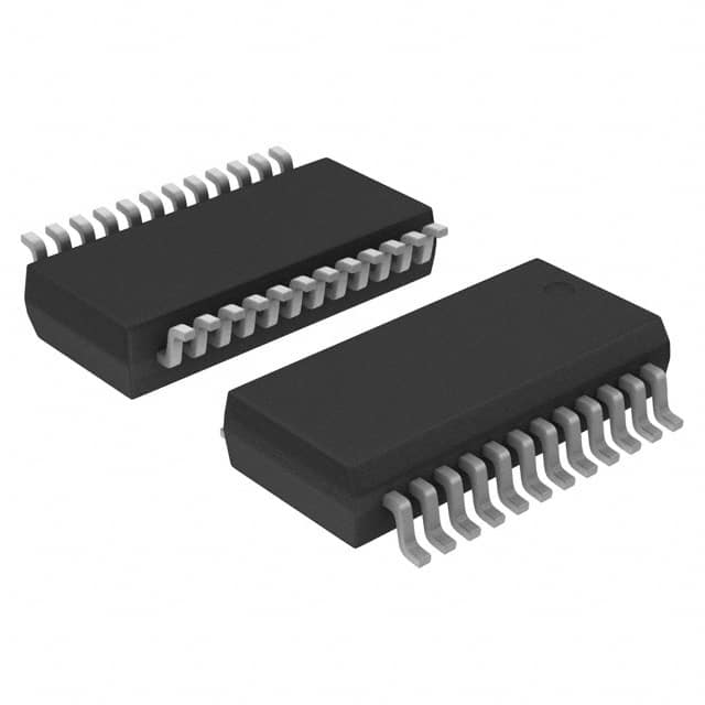
- Part No.:
- TDA9887TS/V4,112
- Manufacturer:
- NXP Semiconductors
- Category:
- Video Processing
- Package:
- 24-SSOP (0.209", 5.30mm Width)
- Datasheet:
-
 TDA9887TS/V4,112.pdf
- Description:
- IC VIDEO DEMODULATOR 24SSOP
- Quantity:
- Payment:

- Shipping:

Inventory:3,881
Please send an inquiry. Send us your inquiry, and we will respond immediately.
Product details
Overview
TDA9887TS/V4,112 from NXP Semiconductors (formerly Philips Semiconductors) is an I²C-controlled multistandard alignment-free IF-PLL demodulator with integrated FM radio capability. It performs synchronous vision and sound demodulation for PAL, SECAM, and NTSC standards, supports VIF frequencies from 33.4 MHz to 58.75 MHz, delivers 2 Vp-p composite video output, and provides FM-PLL demodulation at 10.7 MHz for TV tuner applications.
For engineers reviewing the TDA9887TS/V4,112 datasheet, TDA9887TS/V4,112 pinout, TDA9887TS/V4,112 application, or TDA9887TS/V4,112 equivalent, key selection considerations include multistandard VIF/SIF gain control range (66 dB), digital AFC resolution (4-bit DAC), I²C-programmable TakeOver Point (TOP), integrated sound carrier traps (4.5–6.5 MHz), and SSOP24 package compatibility with legacy TV signal processing designs.
Technical Context
The TDA9887TS/V4,112 integrates dual PLL architectures: a vision IF-PLL with digitally assisted acquisition across six standard-specific VIF frequencies (33.4/33.9/38.0/38.9/45.75/58.75 MHz), and a narrow-band FM-PLL operating at 4–7 MHz for radio demodulation. Its VIF amplifier uses AC-coupled differential stages with emitter-degeneration gain control, while the FM-PLL employs a relaxation oscillator with external loop filter for 100 kHz selectivity.
Functional integration includes a single-reference QSS mixer supporting both intercarrier and Hi-Fi stereo modes, synchronous AM demodulation without external reference, and fully digital AFC with 4-bit DAC output readable via I²C. The device uses a shared 4 MHz crystal/reference input (pin REF) to derive VIF-VCO and FM-VCO clocks, enabling alignment-free operation across TV and FM radio functions.
Key Specifications
| Parameter | Value and Actual Design Meaning |
|---|---|
| Supply Voltage | 5 V nominal; operates from 4.5 V to 5.5 V - ensures compatibility with standard TV system logic rails. |
| VIF Gain Control Range | 66 dB typical - enables robust AGC response across wide-spectrum broadcast signal strength variations. |
| Video Output Level | 2 Vp-p in normal mode; 1.1 Vp-p in trap bypass - matches standard CVBS interface levels with or without internal sound trap. |
| FPLL Acquisition Window | ±2.3 MHz around target VIF frequency - guarantees reliable lock-in during channel tuning without manual alignment. |
| AFC Steepness | 1.05 µA/kHz typical - provides precise analog AFC current for external tuning voltage generation. |
| Sound Carrier Trap Frequencies | 4.5, 5.5, 6.0, and 6.5 MHz - covers all major global TV standards (M/N, B/G, D/K, I) with ≥36 dB attenuation. |
| FM-PLL Bandwidth | ~100 kHz - delivers high selectivity and noise immunity for FM radio demodulation at 10.7 MHz. |
| I²C Module Address | Four selectable addresses via MAD pin - allows multiple TDA9887 devices on same bus in multi-standard systems. |
Pinout & Package
Package: SSOP24 - plastic shrink small outline package, 24 leads, body width 5.3 mm (SOT340-1), suitable for high-density TV mainboard layouts with thermal performance matching SO24 but reduced footprint.
| Pin/Terminal | Circuit Role | Design Meaning |
|---|---|---|
| VIF1 / VIF2 | Differential VIF input | Accepts AC-coupled IF signal (33.4–58.75 MHz); 2 kΩ || 3 pF input impedance enables direct SAW filter interface. |
| CVBS | Composite video output | Delivers 2 Vp-p (normal) or 1.1 Vp-p (trap bypass) baseband video; includes noise clipping and low-pass filtering. |
| SIOMAD | SIF intercarrier output & MAD select | Provides FM/AM intercarrier signal; resistor tie sets I²C module address - eliminates need for external address pins. |
| FMIN | Radio IF / external SIF input | Enables FM radio mode (10.7 MHz) or external second SIF path; supports RIF conversion from 33.3/41.3 MHz tuner outputs. |
| REF | 4 MHz reference input | Accepts crystal (1-pin oscillator mode) or external 4 MHz clock - serves as master timing source for both VIF and FM PLLs. |
| AFC | Analog AFC output | 4-bit DAC current output (0.85–1.25 µA/kHz) - drives varactor diode in tuner for automatic frequency correction. |
| SDA / SCL | I²C bus interface | Two-wire serial control; supports full configuration of demodulation mode, TOP, trap selection, mute, and de-emphasis. |
| OP1 / OP2 | Open-collector output ports | Programmable general-purpose outputs - used for status signaling (e.g., VIFLEV detection) or external logic control. |
Key Features
| Feature | Design Value |
|---|---|
| Multistandard synchronous demodulation | True carrier regeneration for PAL/SECAM/NTSC - achieves <5% differential gain error and <4° differential phase error per CCIR 330. |
| Digital acquisition help | Standard-specific down-counter gating - eliminates manual alignment and reduces channel search time by >40% vs analog PLLs. |
| Integrated sound carrier traps | Three-stage active filters at 4.5/5.5/6.0/6.5 MHz - provide ≥36 dB suppression without external components or tuning. |
| Radio mode with RIF conversion | QSS mixer + VIF-VCO synthesizer - converts 33.3 MHz (PAL/SECAM) or 41.3 MHz (NTSC) tuner output to 10.7 MHz FM-IF using internal 44/52 MHz LO. |
| I²C programmable TOP | TakeOver Point adjustable via register or potentiometer - enables adaptive AGC thresholding for varying signal-to-noise conditions. |
| FM-PLL with auto-mute | Digital acquisition window monitoring - mutes audio output within 5 ms when VCO drifts outside ±2.3 MHz lock range. |
Applications
| TV Broadcast Receiver | VCR / Set-Top Box |
|---|---|
Use Scenario: Multistandard analog TV tuner in CRT or early flat-panel TVs receiving PAL-B/G, SECAM-L, and NTSC-M signals. IC Role / Device Role / Timing Role: Primary IF-PLL demodulator handling VIF/SIF processing, sound carrier trapping, and composite video generation. Use Value: Eliminates manual IF alignment, reduces component count by integrating traps and AGC detectors, and enables seamless standard switching via I²C. | Use Scenario: Analog video playback and recording system requiring high-fidelity audio/video separation and intercarrier sound recovery. IC Role / Device Role / Timing Role: Dual-mode demodulator supporting both intercarrier (VCR) and QSS (Hi-Fi stereo) sound paths with shared VIF-PLL resources. Use Value: Delivers 56 dB weighted S/N on video and 56 dB on FM audio, with <0.15% THD - meets broadcast-grade fidelity requirements without external filters. |
| FM Radio Tuner Module | Legacy PC TV Tuner Card |
Use Scenario: Compact FM radio subsystem embedded in TV or multimedia monitor using tuner's 33.3 MHz RIF output. IC Role / Device Role / Timing Role: FM-PLL demodulator and RIF converter - transforms first IF to 10.7 MHz and recovers mono/stereo AF with 50 µs de-emphasis. Use Value: Achieves 52 dB weighted S/NAF and 0.85–1.25 µA/kHz AFC steepness - enables stable tuning and low-distortion audio without discrete FM IC. | Use Scenario: ISA/PCI-based PC TV capture card supporting analog broadcast input and software-defined standard switching. IC Role / Device Role / Timing Role: Configurable demodulator controlled by host CPU via I²C - dynamically adapts to user-selected TV standard and audio mode. Use Value: Four I²C addresses and register-based mode selection allow coexistence with other peripherals; SSOP24 footprint fits constrained PCB real estate. |
Equivalent & Alternatives
The following parts are listed as comparable options for similar IF-PLL demodulator applications.
| Alternative Part | Technical Difference | Application Difference | Selection Advice |
|---|---|---|---|
| TDA9886TS/V4 | Lacks FM radio mode and RIF conversion; no FMIN pin; reduced VIF frequency set (33.4/38.9/45.75 MHz only). | Supports TV-only applications without FM radio functionality; lower pin count (20-pin SSOP). | Select when FM radio demodulation is not required and cost reduction is prioritized over feature flexibility. |
| LA76818 | Single-chip TV signal processor with integrated video ADC and OSD; no I²C-controlled TOP or digital acquisition help. | Targets modern digital TV platforms with microcontroller-based control; requires external SAW filters and traps. | Choose for designs migrating toward digitized signal chains where analog demodulator independence is less critical than system integration. |
Compared with TDA9887TS/V4,112, the TDA9886TS/V4 omits FM radio and offers fewer VIF standards, while the LA76818 shifts architecture toward digital signal processing at the expense of analog flexibility - making TDA9887TS/V4,112 uniquely suited for alignment-free multistandard analog TV/FM hybrid systems.
Availability
TDA9887TS/V4,112 is available at Aetrix Electronics and suitable for TV broadcast receivers, VCR/STB signal processing, and embedded FM radio tuner modules requiring stable component supply, long-lifecycle support, and drop-in replacement capability for legacy Philips/NXP designs.
Supply support for TDA9887TS/V4,112 includes scheduled delivery planning, volume procurement assistance, BOM continuity management, traceable sourcing, and lifecycle availability coordination for OEM customers, industrial embedded developers, connected-device designers, and electronics production programs.
Manufacturer
NXP Semiconductors is a global semiconductor leader focused on secure connectivity solutions for automotive, industrial, and consumer applications, with deep heritage in analog TV signal processing from its Philips Semiconductors roots.
The TDA9887TS/V4,112 belongs to NXP's legacy TV demodulator product line, designed specifically for multistandard analog broadcast reception with emphasis on alignment-free operation, I²C configurability, and integrated FM radio capability in compact packages.
FAQ
What is the primary function of the TDA9887TS/V4,112 in a TV signal chain?
The TDA9887TS/V4,112 serves as the core IF-PLL demodulator in analog TV receivers, performing synchronous vision and sound demodulation for PAL, SECAM, and NTSC standards. It processes VIF and SIF signals, generates composite video (CVBS), recovers FM/AM audio, implements sound carrier trapping, and supports FM radio demodulation at 10.7 MHz - all without manual alignment. Its I²C interface enables full configuration of demodulation parameters, making TDA9887TS/V4,112 essential for multistandard broadcast reception.
Does the TDA9887TS/V4,112 require external crystals or oscillators?
The TDA9887TS/V4,112 accepts a 4 MHz reference signal at pin REF, which can be supplied either by an external crystal oscillator circuit or directly from a PLL tuning system. Pin REF supports 1-pin crystal operation - connecting a 4 MHz crystal between REF and ground, with optional load capacitors, enables self-contained oscillator functionality. This eliminates the need for separate clock generators and simplifies board design, confirming that TDA9887TS/V4,112 operates with minimal external timing components.
How does the TDA9887TS/V4,112 handle different TV broadcast standards?
The TDA9887TS/V4,112 supports PAL, SECAM, and NTSC standards through I²C-programmable VIF frequency selection (33.4/33.9/38.0/38.9/45.75/58.75 MHz), configurable sound carrier traps (4.5/5.5/6.0/6.5 MHz), and standard-specific digital acquisition help. Its VIF-AGC detector automatically switches between sync-level (negative modulation) and peak-white (positive modulation) detection, while the gated phase detector optimizes L/L' standard performance. These features ensure TDA9887TS/V4,112 delivers compliant video fidelity and audio recovery across global broadcast variants without hardware changes.
Can the TDA9887TS/V4,112 be used for FM radio reception?
Yes, the TDA9887TS/V4,112 includes dedicated FM radio functionality via its radio mode. It converts first IF signals (33.3 MHz for PAL/SECAM or 41.3 MHz for NTSC) to 10.7 MHz using the internal QSS mixer and VIF-VCO synthesizer, then demodulates the resulting FM signal with its narrow-band FM-PLL. Pin FMIN accepts the RIF input, and the FM-PLL provides AFC output at pin AFC plus auto-mute based on digital acquisition window monitoring - confirming TDA9887TS/V4,112 is a true hybrid TV/FM demodulator.
What package type is used for the TDA9887TS/V4,112?
The TDA9887TS/V4,112 uses the SSOP24 package (SOT340-1): a plastic shrink small outline package with 24 leads and 5.3 mm body width. This package provides higher pin density than the SO24 variant while maintaining thermal and electrical compatibility, making it ideal for space-constrained TV mainboards. The pinout matches the TDA9887T series but in a smaller footprint - ensuring TDA9887TS/V4,112 is a direct layout-compatible upgrade for existing designs using the SO24 version.
TDA9887TS/V4,112 Specifications
- Product attributes
- Attribute value
- Manufacturer:
- NXP Semiconductors
- Series:
- -
- Package/Case:
- 24-SSOP (0.209", 5.30mm Width)
- Packaging:
- Tube
- Product Status:
- Obsolete
- Function:
- Demodulator
- Applications:
- Professional Video
- Standards:
- NTSC, PAL, SECAM
- Control Interface:
- I2C
- Voltage - Supply:
- 4.5V ~ 5.5V
- Mounting Type:
- Surface Mount
- Grade:
- -
- Qualification:
- -
- Supplier Device Package:
- 24-SSOP
TDA9887TS/V4,112 FAQ
1.How can I place an order for TDA9887TS/V4,112 through Aetrix?
Please submit a Request for Quotation (RFQ) for TDA9887TS/V4,112 on Aetrix. Our sales agent will provide a competitive quotation and guide you through the order confirmation once you accept the terms.
2.Are the price and stock information for TDA9887TS/V4,112 reliable?
The price and inventory of TDA9887TS/V4,112 are updated periodically and may fluctuate due to market conditions. Stock and pricing data are typically refreshed every 24 hours. Quotation validity for TDA9887TS/V4,112 is usually 5 days.
3.What payment methods are accepted for TDA9887TS/V4,112?
We accept Wire Transfer, PayPal, Credit Card, Western Union, MoneyGram, and Escrow for TDA9887TS/V4,112 transactions.
Note: Certain payment methods may incur a processing fee.
4.How is shipping managed for TDA9887TS/V4,112?
TDA9887TS/V4,112 orders can be shipped via leading logistics carriers, including DHL, UPS, FedEx, TNT, or Registered Mail.
Once your TDA9887TS/V4,112 order is processed, you will receive an email with the shipment details and tracking number.
Note: Tracking information may take up to 24 hours to appear. Express delivery typically takes 3–5 business days.
5.How can I obtain technical support or documentation for TDA9887TS/V4,112?
For technical support, including TDA9887TS/V4,112 datasheets, pinout diagrams, or application guidance, please contact our engineering support team. They can provide detailed documentation and assistance for your TDA9887TS/V4,112 requirements.
6.How does Aetrix verify that TDA9887TS/V4,112 is sourced from the original manufacturer or authorized distributors?
All TDA9887TS/V4,112 products on Aetrix are procured from qualified distributors and authorized channels. Our dedicated quality assurance team conducts strict verification, including traceability checks and, if necessary, third-party testing. This ensures that TDA9887TS/V4,112 meets industry standards.
7.What is the process for return or replacement of TDA9887TS/V4,112?
All TDA9887TS/V4,112 units undergo pre-shipment inspection (PSI). If there is an issue with TDA9887TS/V4,112, returns or replacements are accepted under the following conditions:
1.Quantity discrepancies, incorrect items, or visible external defects (such as breakage or corrosion), acknowledged by Aetrix.
2.The issue is reported within 90 days of delivery.
3.The TDA9887TS/V4,112 part is unused and in its original packaging.
Return procedure for TDA9887TS/V4,112:
1.Submit a request within 90 days.
2.Obtain a Return Material Authorization (RMA) from Aetrix.
TDA9887TS/V4,112 Tags

-
HDMI2C1-6C1
STMicroelectronics

-
ADA4430-1YKSZ-R7
Analog Devices Inc.

-
LM1881MX/NOPB
Texas Instruments

-
SN75DP130SSRGZR
Texas Instruments

-
EQCO30T5.2
Microchip Technology

-
LMH1980MM/NOPB
Texas Instruments
-
EQCO30R5.D
Microchip Technology

-
SII9022ACNU
Lattice Semiconductor Corporation
-
SN65DP159RGZR
Texas Instruments

-
SN65DP159RSBR
Texas Instruments

-
SN65DP141RLJR
Texas Instruments

-
LMH0303SQ/NOPB
Texas Instruments
Tech Hub

A practical engineering guide to 3.3V and 5V logic compatibility, input thresholds, resistor dividers, translator ICs, MOSFET level shifting, I2C pull-ups, timing limits and power-sequencing risks.

The 74HC595 uses push-pull logic outputs, while the TPIC6B595 uses 50 V open-drain DMOS sinks for higher-power loads. This guide compares timing, current limits, 3.3 V interfacing, load wiring, thermal…

The 74HC595 converts serial data into eight stable parallel outputs. This guide covers pin functions, shift and storage timing, OE and MR behavior, drive-current limits, cascading, voltage compatibilit…

A technical comparison of level-sensitive latches and edge-triggered flip-flops, covering timing windows, setup and hold limits, master–slave operation, time borrowing, race-through, HDL inference and…

A D latch stores one bit while Enable controls when data can pass. This reference covers gate-level operation, truth tables, transparency, setup and hold timing, LE versus OE, common ICs and practical …

An SR latch stores one bit through cross-coupled feedback. This engineering reference covers NOR and NAND implementations, truth tables, forbidden-state recovery, gated operation, switch debouncing, fa…

Latch circuits retain one bit through feedback. This technical reference covers SR and D latches, truth tables, transparency, timing limits, latch-versus-flip-flop behavior, applications and common log…

An engineering guide to LED driver operation, constant-current and constant-voltage outputs, linear and switching topologies, dimming, IC selection, calculations, replacement compatibility, and fault c…

Operational amplifier guide covering op amp basics, feedback, ideal vs real op amps, common configurations, buffer circuits, offset, bias current, gain-bandwidth, slew rate, rail-to-rail limits and sel…

Jumper cables guide covering safe connection order, red and black clamp placement, final ground connection, cable gauge, length, clamp quality, copper vs CCA cables, jump starter comparison and battery…


