
 My Inquiry
 My Account


NXP Semiconductors TEA1721BDB1065,598
- Part No.:
- TEA1721BDB1065,598
- Manufacturer:
- NXP Semiconductors
- Package:
- Datasheet:
-
 TEA1721BDB1065,598.pdf
- Description:
- EVAL BOARD FOR TEA1721
- Quantity:
- Payment:

- Shipping:

Inventory:2,914
Please send an inquiry. Send us your inquiry, and we will respond immediately.
Product details
Overview
TEA1721BDB1065,598 from NXP is a GreenChip SMPS controller IC with integrated 700 V high-voltage MOSFET, designed for primary-side regulated flyback converters up to 5 W. It delivers <10 mW no-load power consumption, supports USB CC/CV charging, and eliminates optocouplers via primary-sensed voltage control - used in mobile USB chargers and smart meter power supplies.
For engineers reviewing the TEA1721BDB1065,598 datasheet, TEA1721BDB1065,598 pinout, TEA1721BDB1065,598 application, or TEA1721BDB1065,598 equivalent, key selection criteria include its SO7 package, 430 Hz burst frequency, 50.5 kHz max switching frequency, EEPROM-programmable burst modes, and compliance with Energy Star 2.0 and USB battery charging standards.
Technical Context
The TEA1721BDB1065,598 implements primary-side regulation using demagnetization detection and cable impedance compensation (0.3 Ω), enabling accurate CV/CC output without secondary feedback. Its architecture integrates active HV start-up, zero-current switching during normal operation, and soft-start via peak current reduction.
It operates in discontinuous conduction mode (DCM) with guaranteed demagnetization protection, includes OVP with auto-restart, UVLO with clamp, OTP, FB open/short protection, and jittering for EMI reduction - all while maintaining min fsw >22 kHz to avoid audible noise.
Key Specifications
| Parameter | Value and Actual Design Meaning |
|---|---|
| Max Output Power | 5 W - rated for compact, low-power AC/DC adapters targeting USB charging and white goods auxiliary supplies. |
| No-Load Power Consumption | <10 mW - meets Energy Star 2.0 and EPA Tier 2 requirements without external bleeder resistors. |
| Switching Frequency | Up to 50.5 kHz - enables small magnetics and high efficiency across load range while staying above audible range. |
| Burst Frequency | 430 Hz - EEPROM-programmable; balances transient response and ultra-low standby power. |
| Cable Compensation | 0.3 Ω - compensates for voltage drop in USB cables to maintain ±5% CV accuracy at device port. |
| Integrated Switch | 700 V HV MOSFET - supports universal mains (85–265 VAC) without external HV starter circuitry. |
| Protection Features | OVP, UVLO, OTP, FB open/short, demag protection, safe restart - ensures robust operation in unattended consumer/industrial systems. |
Pinout & Package
TEA1721BDB1065,598 is housed in a halogen-free, RoHS-compliant SO7 package with HV spacing optimized for mains-referenced primary-side layouts.
| Pin/Terminal | Circuit Role | Design Meaning |
|---|---|---|
| VDD | Supply input / HV start-up node | Accepts rectified mains; internal HV current source enables start-up without bleeder resistor. |
| SW | Drain of integrated 700 V MOSFET | Connects directly to transformer primary; handles full HV switching stress. |
| GND | Power and signal reference | Common return for control logic and power switch; requires low-inductance layout. |
| FB | Primary-side feedback input | Samples reflected auxiliary winding voltage for regulation; includes open/short fault detection. |
| CS | Current sense input | Monitors MOSFET source current for peak current limiting, soft-start, and OCP. |
| DRV | Gate drive output | Internal driver for integrated MOSFET; not accessible externally. |
| NC | No connect | Internally unused pin; must remain floating per datasheet layout guidelines. |
Key Features
| Feature | Design Value |
|---|---|
| Primary-side regulation | Eliminates optocoupler and TL431, reducing BOM count by ≥3 components and improving reliability. |
| EEPROM-programmable burst mode | Enables tuning of 430 Hz burst frequency to optimize trade-off between no-load power and load-step response. |
| Cable impedance compensation | Applies 0.3 Ω correction to maintain ±5% CV accuracy at USB device connector under varying cable lengths. |
| Active HV start-up | Integrates HV current source - removes external 1 MΩ bleeder resistor and associated power loss. |
| EMI jitter function | Spreads switching spectrum to reduce peak emissions, easing compliance with CISPR 22 Class B without Y-cap. |
Applications
| Mobile USB Charging | Smart Meter Auxiliary Supply |
|---|---|
Use Scenario: Wall adapter powering smartphones via USB-A port with CC/CV profile. IC Role / Device Role / Timing Role: Primary-side SMPS controller managing flyback regulation, cable compensation, and USB charging handshake timing. Use Value: Delivers <10 mW no-load power and ±5% CV accuracy at device port - meeting Energy Star 2.0 and USB-IF requirements. | Use Scenario: On-board 5 V/100 mA auxiliary supply for metrology MCU and RTC in utility smart meters. IC Role / Device Role / Timing Role: Standalone AC/DC controller providing isolated, regulated DC with high reliability over 15+ year field life. Use Value: Integrated OVP, OTP, and safe-restart ensure fail-safe behavior during grid transients and long-term unattended operation. |
| White Goods Control Power | Industrial IoT Sensor Node Supply |
Use Scenario: Low-power auxiliary supply for display, touch panel, and MCU in refrigerators or washing machines. IC Role / Device Role / Timing Role: Flyback controller delivering stable 3.3 V/5 V from mains, with demagnetization-based DCM control. Use Value: SO7 footprint and <30-component BOM enable compact, cost-optimized PCB layout in space-constrained appliance control boards. | Use Scenario: Mains-powered sensor gateway requiring ultra-low standby for remote monitoring in factory environments. IC Role / Device Role / Timing Role: Primary-regulated SMPS providing always-on 3.3 V rail with <10 mW idle draw and brown-out immunity. Use Value: UVLO with clamp and auto-restart on fault allow continuous operation despite unstable industrial AC input conditions. |
Equivalent & Alternatives
The following parts are listed as comparable options for similar SMPS controller applications.
| Alternative Part | Technical Difference | Application Difference | Selection Advice |
|---|---|---|---|
| TEA1721AT/N1,598 | No cable compensation (0 Ω); fixed 430 Hz burst; same SO7 package and 5 W rating. | Targeted at general-purpose adapters where USB cable drop is negligible or managed externally. | Select when cable compensation is unnecessary and BOM simplicity is prioritized over port-level CV accuracy. |
| MP172GJ-Z | Monolithic 650 V controller (no integrated MOSFET); requires external HV FET; supports up to 6 W. | Used where design flexibility (e.g., custom MOSFET selection) outweighs integration benefits. | Choose when thermal management or specific Rds(on) optimization demands discrete power switch implementation. |
Compared with TEA1721BDB1065,598, TEA1721AT/N1,598 offers identical topology support but lacks cable compensation - limiting USB port accuracy - while MP172GJ-Z trades integration for design flexibility, requiring external HV FET and increasing component count but enabling higher efficiency tuning.
Availability
TEA1721BDB1065,598 is available at Aetrix Electronics and suitable for mobile USB chargers, smart meter auxiliary supplies, and white goods control power applications requiring stable component supply, long lifecycle support, and regulatory compliance.
Supply support for TEA1721BDB1065,598 includes scheduled delivery planning, volume procurement assistance, BOM continuity management, traceable sourcing, and lifecycle availability coordination for OEM customers, industrial embedded developers, connected-device designers, and electronics production programs.
Manufacturer
NXP Semiconductors is a global semiconductor company focused on secure connectivity solutions for automotive, industrial, and IoT markets.
The TEA172x product line delivers highly integrated, low-noise, ultra-low-standby SMPS controllers for cost-sensitive, safety-critical AC/DC power conversion in consumer and industrial equipment.
FAQ
What is the maximum output power supported by the TEA1721BDB1065,598?
The TEA1721BDB1065,598 is rated for up to 5 W continuous output power in flyback configurations. This rating reflects its integrated 700 V MOSFET's safe operating area and thermal design envelope under typical ambient conditions. It is not rated for 11 W operation - that capability belongs to the TEA1723 variant. The 5 W limit ensures reliable DCM operation and compliance with no-load and efficiency targets.
Does the TEA1721BDB1065,598 support USB Battery Charging specification compliance?
Yes, the TEA1721BDB1065,598 supports USB Battery Charging (BC) 1.2 compliance through its built-in CC/CV control loop and cable impedance compensation. It delivers ±5% constant voltage and ±10% constant current accuracy at the USB port when configured per NXP application notes. This enables direct use in certified mobile USB chargers without secondary-side feedback components.
What package type and pin count does the TEA1721BDB1065,598 use?
The TEA1721BDB1065,598 uses a 7-pin SO (Small Outline) package with HV creepage spacing - designated SO7 in NXP documentation. All pins are surface-mount compatible, and the NC (no-connect) pin must remain unconnected. The package is halogen-free and RoHS compliant, meeting IPC/JEDEC J-STD-020 moisture sensitivity level 3.
How does the TEA1721BDB1065,598 achieve <10 mW no-load power consumption?
The TEA1721BDB1065,598 achieves <10 mW no-load power via integrated active HV start-up (eliminating bleeder resistors), burst-mode operation at 430 Hz, and ultra-low quiescent current in sleep state. Its architecture disables non-essential circuitry during light load, and the EEPROM-programmable burst frequency allows fine-tuning to minimize idle draw without sacrificing wake-up response time.
Is the TEA1721BDB1065,598 pin-compatible with other TEA172x variants like TEA1721AT/N1,598?
Yes, the TEA1721BDB1065,598 is pin-compatible with TEA1721AT/N1,598 and other SO7-packaged TEA1721 variants. All share identical pinout, package dimensions, and thermal pad configuration. However, internal EEPROM settings differ - specifically, TEA1721BDB1065,598 is programmed for 0.3 Ω cable compensation, whereas TEA1721AT/N1,598 defaults to 0 Ω. Firmware or hardware-level verification is required before substitution.
TEA1721BDB1065,598 Specifications
- Product attributes
- Attribute value
- Manufacturer:
- NXP Semiconductors
- Series:
- -
- Packaging:
- Box
- Product Status:
- Active
- Main Purpose:
- AC/DC, Primary Side
- Outputs and Type:
- 2 Isolated Outputs
- Voltage - Output:
- 5 W
- Current - Output:
- -3.3V, -12V
- Voltage - Input:
- 400mA, 400mA
- Regulator Topology:
- 85 ~ 265 VAC
- Frequency - Switching:
- Flyback
- Contents:
- 50kHz
- Utilized IC / Part:
- Board(s)
- Power - Output:
- TEA1721
TEA1721BDB1065,598 FAQ
1.How can I place an order for TEA1721BDB1065,598 through Aetrix?
Please submit a Request for Quotation (RFQ) for TEA1721BDB1065,598 on Aetrix. Our sales agent will provide a competitive quotation and guide you through the order confirmation once you accept the terms.
2.Are the price and stock information for TEA1721BDB1065,598 reliable?
The price and inventory of TEA1721BDB1065,598 are updated periodically and may fluctuate due to market conditions. Stock and pricing data are typically refreshed every 24 hours. Quotation validity for TEA1721BDB1065,598 is usually 5 days.
3.What payment methods are accepted for TEA1721BDB1065,598?
We accept Wire Transfer, PayPal, Credit Card, Western Union, MoneyGram, and Escrow for TEA1721BDB1065,598 transactions.
Note: Certain payment methods may incur a processing fee.
4.How is shipping managed for TEA1721BDB1065,598?
TEA1721BDB1065,598 orders can be shipped via leading logistics carriers, including DHL, UPS, FedEx, TNT, or Registered Mail.
Once your TEA1721BDB1065,598 order is processed, you will receive an email with the shipment details and tracking number.
Note: Tracking information may take up to 24 hours to appear. Express delivery typically takes 3–5 business days.
5.How can I obtain technical support or documentation for TEA1721BDB1065,598?
For technical support, including TEA1721BDB1065,598 datasheets, pinout diagrams, or application guidance, please contact our engineering support team. They can provide detailed documentation and assistance for your TEA1721BDB1065,598 requirements.
6.How does Aetrix verify that TEA1721BDB1065,598 is sourced from the original manufacturer or authorized distributors?
All TEA1721BDB1065,598 products on Aetrix are procured from qualified distributors and authorized channels. Our dedicated quality assurance team conducts strict verification, including traceability checks and, if necessary, third-party testing. This ensures that TEA1721BDB1065,598 meets industry standards.
7.What is the process for return or replacement of TEA1721BDB1065,598?
All TEA1721BDB1065,598 units undergo pre-shipment inspection (PSI). If there is an issue with TEA1721BDB1065,598, returns or replacements are accepted under the following conditions:
1.Quantity discrepancies, incorrect items, or visible external defects (such as breakage or corrosion), acknowledged by Aetrix.
2.The issue is reported within 90 days of delivery.
3.The TEA1721BDB1065,598 part is unused and in its original packaging.
Return procedure for TEA1721BDB1065,598:
1.Submit a request within 90 days.
2.Obtain a Return Material Authorization (RMA) from Aetrix.
TEA1721BDB1065,598 Tags
-
DFR0571
DFRobot
-
DFR0379
DFRobot
-
DFR0205
DFRobot
-
1385
Adafruit Industries LLC
-
COM-15208
SparkFun Electronics
-
1944
Adafruit Industries LLC
-
2465
Adafruit Industries LLC
-
DC2468A
Analog Devices Inc.
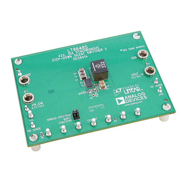
-
DC2841A
Analog Devices Inc.

-
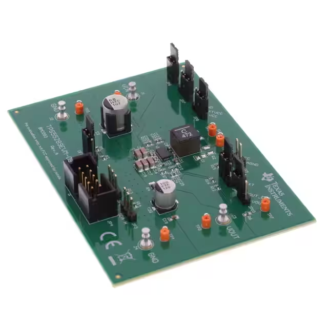
TPS552892EVM-111
Texas Instruments
-
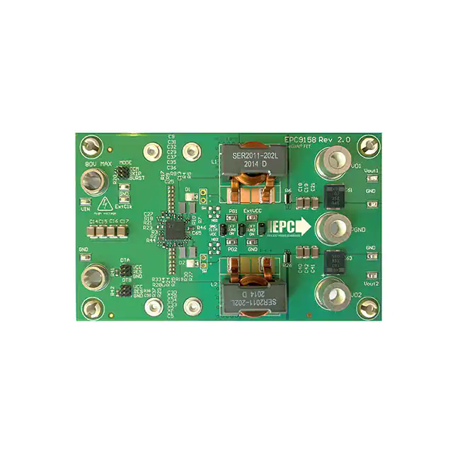
TPS55289EVM-093
Texas Instruments
-
EPC9158
EPC
Tech Hub

A practical engineering guide to 3.3V and 5V logic compatibility, input thresholds, resistor dividers, translator ICs, MOSFET level shifting, I2C pull-ups, timing limits and power-sequencing risks.

The 74HC595 uses push-pull logic outputs, while the TPIC6B595 uses 50 V open-drain DMOS sinks for higher-power loads. This guide compares timing, current limits, 3.3 V interfacing, load wiring, thermal…

The 74HC595 converts serial data into eight stable parallel outputs. This guide covers pin functions, shift and storage timing, OE and MR behavior, drive-current limits, cascading, voltage compatibilit…

A technical comparison of level-sensitive latches and edge-triggered flip-flops, covering timing windows, setup and hold limits, master–slave operation, time borrowing, race-through, HDL inference and…

A D latch stores one bit while Enable controls when data can pass. This reference covers gate-level operation, truth tables, transparency, setup and hold timing, LE versus OE, common ICs and practical …

An SR latch stores one bit through cross-coupled feedback. This engineering reference covers NOR and NAND implementations, truth tables, forbidden-state recovery, gated operation, switch debouncing, fa…

Latch circuits retain one bit through feedback. This technical reference covers SR and D latches, truth tables, transparency, timing limits, latch-versus-flip-flop behavior, applications and common log…

An engineering guide to LED driver operation, constant-current and constant-voltage outputs, linear and switching topologies, dimming, IC selection, calculations, replacement compatibility, and fault c…

Operational amplifier guide covering op amp basics, feedback, ideal vs real op amps, common configurations, buffer circuits, offset, bias current, gain-bandwidth, slew rate, rail-to-rail limits and sel…

Jumper cables guide covering safe connection order, red and black clamp placement, final ground connection, cable gauge, length, clamp quality, copper vs CCA cables, jump starter comparison and battery…


