
 My Inquiry
 My Account


NXP Semiconductors TEA19051BAAT/1J
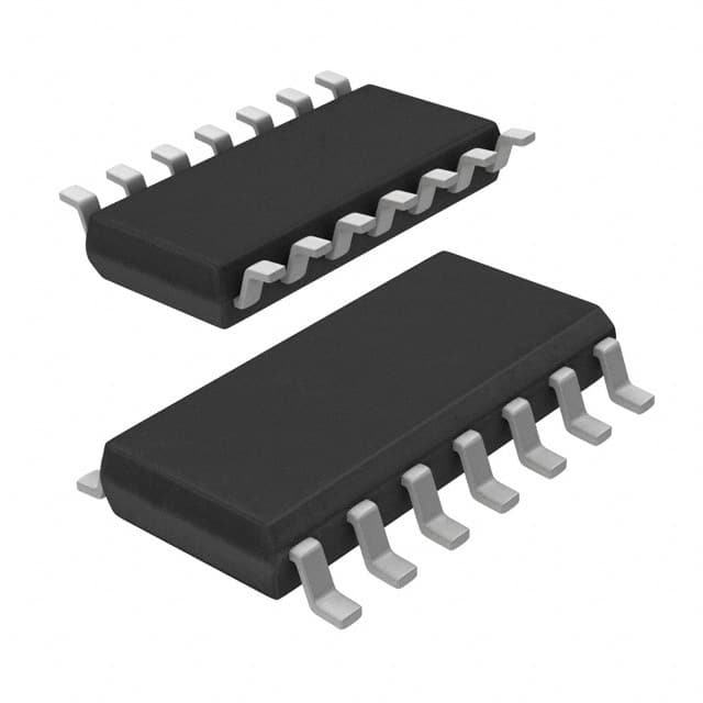
- Part No.:
- TEA19051BAAT/1J
- Manufacturer:
- NXP Semiconductors
- Category:
- Controllers
- Package:
- 14-SOIC (0.154", 3.90mm Width)
- Datasheet:
-
 TEA19051BAAT/1J.pdf
- Description:
- IC USB CONTROLLER 14SO
- Quantity:
- Payment:

- Shipping:

Inventory:4,480
Please send an inquiry. Send us your inquiry, and we will respond immediately.
Product details
Overview
TEA19051BAAT/1J from NXP Semiconductors is a secondary-side USB-PD 3.0/PPS and QC4+ controller IC for AC-DC SMPS, supporting CV/CC regulation with ±2 % output voltage and current accuracy, 2.9–21 V programmable output range, and integrated USB-C CC1/CC2 PHY, DP/DM interface, and NMOS gate driver (SW pin). It enables compact, CoC Tier-2/EuP Lot6-compliant 65 W+ chargers.
For engineers reviewing the TEA19051BAAT/1J datasheet, TEA19051BAAT/1J pinout, TEA19051BAAT/1J application, or TEA19051BAAT/1J equivalent, key selection considerations include its hardware-enforced protections (OTP, OVP, OSP), MTP-programmable PDOs (up to 7, including 4 PPS), dual GPIO temperature sensing, and single-optocoupler feedback architecture.
Technical Context
The TEA19051BAAT/1J implements a digitally controlled analog CV/CC loop: VSNS senses output voltage via resistor divider (MTP-matched ratios: 1/2.5, 1/5.476, or 1/8.325), while ISNS monitors current through an external sense resistor (2–22 mΩ) amplified 50× internally. Regulation commands are executed via USB-PD (CC1/CC2) or QC (DP/DM), with DAC resolution of 12-bit (voltage) and 10-bit (current).
Its protection architecture is fully hardware-based - including adaptive OVP/UVP, OTP (internal + two external), OSP, and soft-short detection on CC1/CC2 - ensuring fail-safe operation independent of firmware execution. The SW pin drives an external NMOS load switch using an internal charge pump (VCC + 6 V), and DISCH provides controlled Vbus discharge to vSafe0V (<0.8 V) per USB-PD spec.
Key Specifications
| Parameter | Value and Actual Design Meaning |
|---|---|
| Output Voltage Range | 2.9 V to 21 V; supports USB-PD PPS and QC3.0/4+ stepwise adjustment (200 mV steps) |
| CV/CC Accuracy | ±2 % full-scale; enables tight compliance with USB-PD 3.0 and QC4+ voltage/current tolerance requirements |
| No-Load Power | <30 mW system-level; meets CoC Tier-2, EuP Lot6, and DOE VI efficiency standards |
| Protocol Support | USB-PD 2.0/3.0 (including PPS), QC2.0/QC3.0/QC4+, BC1.2, USB Type-C v1.3; all implemented in hardware/firmware |
| Protection Architecture | Fully hardware-enforced: OTP (internal + 2 external), OVP/UVP (adaptive), OSP, OSUP, OGP, CC/DP/DM pin overvoltage |
| MTP Memory | Multi-Time Programmable storage for 7 PDOs (4 configurable as PPS), cable compensation, GPIO functions, and safety thresholds |
| Package | SO14 (SOT108-1); 3.9 mm body width, reflow/wave solder compatible, low-cost BOM integration |
Pinout & Package
TEA19051BAAT/1J is housed in a plastic small outline package (SO14, SOT108-1) with 14 leads and 3.9 mm body width, optimized for high-density USB-PD charger designs requiring minimal external components.
| Pin/Terminal | Circuit Role | Design Meaning |
|---|---|---|
| VCC | Supply input | Secondary-side DC supply (up to 21 V); powers internal circuits and triggers UVLO/OVP/UVP based on programmed % of PDO |
| SW | NMOS gate driver | Charge-pump boosted output (VCC + 6 V) directly drives external load switch; ensures safe power path control |
| OPTO | Optocoupler driver | Replaces TL431 cathode; interfaces with primary-side controller (e.g., TEA193x) via single optocoupler for CV/CC feedback |
| GND | Power ground | Main return path for internal digital/analog blocks; separate from SGND to avoid noise coupling in current sensing |
| SGND | Sense ground | Dedicated low-noise ground for ISNS and VSNS; must be connected via independent trace to sense resistor ground |
| DISCH | Fast Vbus discharge sink | Internal low-RON switch discharges output to <0.8 V for USB-PD hard reset; includes millisecond-gated sampling for vSafe0V verification |
| GPIO1 / GPIO2 | Configurable I/O | Support NTC thermistor readout (adapter/cable temp), NTC+OTP, or I²C slave supply; adaptive current sourcing (15/60/240 µA) |
| ISNS | Current sense input | Accepts mV-level drop across external sense resistor (2–22 mΩ); 50× internal gain ensures sub-2.5 V compliance |
| VSNS | Voltage sense input | Monitors scaled-down Vout via MTP-matched resistor divider; sets CV reference with 12-bit DAC precision |
| CC1 / CC2 | USB-C configuration channel | Hardware-based attach/detach detection and USB-PD physical layer (PHY); supports Rp/Rd pull-up/pull-down per USB-C v1.3 |
| DP / DM | QC/BC data interface | Enables Qualcomm QuickCharge 2.0/3.0/4+ negotiation and BC1.2 D+/D− handshake; must be shorted for BC1.2 compliance |
Key Features
| Feature | Design Value |
|---|---|
| Hardware-enforced protections | All critical protections (OTP, OVP, OSP, UVP, OSUP, OGP) implemented in analog/hardware logic - remain active even if MCU stalls |
| Programmable PPS support | Up to 4 of 7 MTP-stored PDOs configurable as Programmable Power Supply (PPS) with 20 mV/50 mA resolution for fine-grained charging control |
| Dual NTC temperature monitoring | GPIO1/GPIO2 independently configured for NTC-based adapter and cable connector temperature sensing with <5 °C error (0–120 °C) |
| Single-optocoupler feedback | Integrates CV/CC regulation, USB-PD/QC protocol handling, and protection into one IC - eliminates need for secondary-side microcontroller or additional isolation |
| Ultra-low no-load consumption | <30 mW system-level standby power achieved via intelligent circuit gating, fast-discharge control, and hardware-detached state management |
Applications
| Smartphone Fast Charging Adapter | USB-C Tablet Power Supply |
|---|---|
|
Use Scenario: 65 W USB-C wall charger delivering PPS 5–20 V/3.25 A to flagship smartphones with dynamic voltage stepping. IC Role / Device Role / Timing Role: Secondary-side USB-PD 3.0 controller managing V/I regulation, CC communication, load switch control, and thermal monitoring. Use Value: Enables single-chip compliance with USB-PD 3.0 PPS and QC4+, reducing BOM count by >5 components versus discrete controller + MCU solutions. |
Use Scenario: Multi-voltage 45 W USB-C power supply for tablets supporting both fixed PDOs (9 V/3 A) and PPS (15 V/3 A) for battery optimization. IC Role / Device Role / Timing Role: Central SMPS regulator coordinating CV/CC transitions, cable compensation, and hardware-based OVP during rapid voltage ramp-down. Use Value: Achieves <30 mW no-load power and ±2 % regulation accuracy without secondary microcontroller, meeting global energy efficiency mandates. |
| Laptop Docking Station Charger | Universal QC/USB-PD Travel Adapter |
|
Use Scenario: 100 W docking station power module supplying negotiated 20 V/5 A to laptops while maintaining backward compatibility with 5 V/3 A legacy devices. IC Role / Device Role / Timing Role: Protocol-aware power manager handling simultaneous USB-PD 3.0 discovery, vendor-defined messages (VDMs), and dynamic PDO selection. Use Value: Supports 7 MTP-programmed PDOs (including 4 PPS) and VID/PID/BDC programming for USB-IF certification and OEM branding. |
Use Scenario: Compact travel adapter supporting QC2.0/3.0/4+, USB-PD 2.0/3.0, and BC1.2 across smartphones, earbuds, and wearables. IC Role / Device Role / Timing Role: Multi-protocol negotiator using DP/DM for QC and CC1/CC2 for USB-PD, with automatic fallback to default 5 V/3 A when no protocol detected. Use Value: Eliminates need for separate QC and USB-PD ICs; MTP allows factory configuration for region-specific PDO sets and safety thresholds. |
Equivalent & Alternatives
The following parts are listed as comparable options for similar USB-PD secondary-side controller applications.
| Alternative Part | Technical Difference | Application Difference | Selection Advice |
|---|---|---|---|
| STUSB4500QTR | USB-PD 3.0 sink-only controller; lacks QC support, CC mode, and integrated SW driver; requires external MCU for full DFP functionality | Targeted at cost-sensitive USB-C accessories where QC compatibility is not required; no PPS or multi-protocol negotiation | Choose STUSB4500QTR only for pure USB-PD sink applications with minimal feature set and lower power density requirements. |
| MPQ4282-AEC1 | Automotive-grade USB-PD 3.0 controller with AEC-Q100 qualification; includes CAN interface but no QC support or MTP-configurable PDOs | Designed for vehicle-mounted chargers requiring automotive reliability; lacks consumer-focused features like BC1.2 or DP/DM QC pins | Select MPQ4282-AEC1 exclusively for automotive infotainment or telematics power systems needing AEC-Q100 compliance and CAN integration. |
Compared with TEA19051BAAT/1J, STUSB4500QTR offers simpler USB-PD sink functionality but no QC or PPS, while MPQ4282-AEC1 adds automotive qualification and CAN at the expense of consumer protocol flexibility and field-programmable PDOs - making TEA19051BAAT/1J the only option supporting full USB-PD 3.0 + QC4+ + BC1.2 in a single SO14 package with hardware-enforced safety.
Availability
TEA19051BAAT/1J is available at Aetrix Electronics and suitable for high-efficiency USB-C fast chargers, universal travel adapters, and laptop docking station power supplies requiring stable component supply, long-term lifecycle support, and certified USB-PD 3.0/PPS implementation.
Supply support for TEA19051BAAT/1J includes scheduled delivery planning, volume procurement assistance, BOM continuity management, traceable sourcing, and lifecycle availability coordination for OEM customers, industrial embedded developers, connected-device designers, and electronics production programs.
Manufacturer
NXP Semiconductors is a global semiconductor leader specializing in secure connectivity solutions for automotive, industrial, and consumer electronics, with deep expertise in power management and USB ecosystem integration.
The TEA19051BAAT/1J belongs to NXP's TEA190xx family of highly integrated secondary-side SMPS controllers, designed specifically to replace TL431-based feedback loops in USB-PD and QC-compliant AC-DC adapters while enabling ultra-low no-load power and hardware-grade safety.
FAQ
What protocols does the TEA19051BAAT/1J support natively?
The TEA19051BAAT/1J natively supports USB Power Delivery 2.0 and 3.0 (including Programmable Power Supply), Qualcomm QuickCharge 2.0/3.0/4+, Battery Charging 1.2, and USB Type-C v1.3. All protocol stacks are implemented in firmware with hardware-accelerated PHY layers on CC1/CC2 and DP/DM pins - no external MCU is required for basic operation of TEA19051BAAT/1J.
How many Power Data Objects (PDOs) can be stored in the TEA19051BAAT/1J MTP memory?
The TEA19051BAAT/1J supports up to seven Power Data Objects stored in its non-volatile Multi-Time Programmable (MTP) memory. Four of these can be configured as Programmable Power Supply (PPS) objects, while the remaining three may be set as fixed PDOs. Each PDO includes independent settings for voltage, current, OCP/CC mode, and cable compensation enablement - all configurable during manufacturing or field programming of TEA19051BAAT/1J.
Does the TEA19051BAAT/1J require an external microcontroller to operate?
No, the TEA19051BAAT/1J does not require an external microcontroller. It integrates an embedded MCU with ROM, RAM, and MTP memory, along with dedicated hardware blocks for USB-PD PHY, QC protocol handling, CV/CC regulation, and protection logic. The TEA19051BAAT/1J operates autonomously as a complete secondary-side controller - only external passive components (resistors, NTCs, sense resistor, optocoupler) and an NMOS load switch are needed for full USB-PD 3.0 + QC4+ functionality.
What is the purpose of the DISCH pin on the TEA19051BAAT/1J?
The DISCH pin on the TEA19051BAAT/1J provides hardware-controlled fast discharge of the Vbus output to meet USB-PD vSafe0V requirements (<0.8 V) during hard resets. It contains an internal low-RON switch that sinks current through an external series resistor. To verify discharge completion, the TEA19051BAAT/1J periodically opens the DISCH switch for 20 µs every millisecond while monitoring actual Vbus voltage - ensuring reliable compliance with USB-PD specification timing and safety thresholds.
Can the TEA19051BAAT/1J be used in both USB-C and USB-A charger designs?
Yes, the TEA19051BAAT/1J supports both USB-C and USB-A topologies. In USB-C designs, CC1/CC2 pins handle plug detection and USB-PD communication. In USB-A configurations, attach/detach detection can be disabled via MTP programming, and the load switch remains closed unless triggered by protection events. DP/DM pins retain full QC2.0/3.0/4+ and BC1.2 functionality regardless of connector type - enabling flexible reuse of TEA19051BAAT/1J across multiple product lines.
TEA19051BAAT/1J Specifications
- Product attributes
- Attribute value
- Manufacturer:
- NXP Semiconductors
- Package/Case:
- 14-SOIC (0.154", 3.90mm Width)
- Programmable:
- Not Verified
- Protocol:
- USB
- Function:
- Controller
- Interface:
- USB
- Standards:
- USB 2.0, USB 3.0
- Voltage - Supply:
- 2.9V ~ 21V
- Current - Supply:
- 3mA
- Operating Temperature:
- -20°C ~ 105°C (TJ)
- Supplier Device Package:
- 14-SO
- Grade:
- -
- Qualification:
- -
TEA19051BAAT/1J FAQ
1.How can I place an order for TEA19051BAAT/1J through Aetrix?
Please submit a Request for Quotation (RFQ) for TEA19051BAAT/1J on Aetrix. Our sales agent will provide a competitive quotation and guide you through the order confirmation once you accept the terms.
2.Are the price and stock information for TEA19051BAAT/1J reliable?
The price and inventory of TEA19051BAAT/1J are updated periodically and may fluctuate due to market conditions. Stock and pricing data are typically refreshed every 24 hours. Quotation validity for TEA19051BAAT/1J is usually 5 days.
3.What payment methods are accepted for TEA19051BAAT/1J?
We accept Wire Transfer, PayPal, Credit Card, Western Union, MoneyGram, and Escrow for TEA19051BAAT/1J transactions.
Note: Certain payment methods may incur a processing fee.
4.How is shipping managed for TEA19051BAAT/1J?
TEA19051BAAT/1J orders can be shipped via leading logistics carriers, including DHL, UPS, FedEx, TNT, or Registered Mail.
Once your TEA19051BAAT/1J order is processed, you will receive an email with the shipment details and tracking number.
Note: Tracking information may take up to 24 hours to appear. Express delivery typically takes 3–5 business days.
5.How can I obtain technical support or documentation for TEA19051BAAT/1J?
For technical support, including TEA19051BAAT/1J datasheets, pinout diagrams, or application guidance, please contact our engineering support team. They can provide detailed documentation and assistance for your TEA19051BAAT/1J requirements.
6.How does Aetrix verify that TEA19051BAAT/1J is sourced from the original manufacturer or authorized distributors?
All TEA19051BAAT/1J products on Aetrix are procured from qualified distributors and authorized channels. Our dedicated quality assurance team conducts strict verification, including traceability checks and, if necessary, third-party testing. This ensures that TEA19051BAAT/1J meets industry standards.
7.What is the process for return or replacement of TEA19051BAAT/1J?
All TEA19051BAAT/1J units undergo pre-shipment inspection (PSI). If there is an issue with TEA19051BAAT/1J, returns or replacements are accepted under the following conditions:
1.Quantity discrepancies, incorrect items, or visible external defects (such as breakage or corrosion), acknowledged by Aetrix.
2.The issue is reported within 90 days of delivery.
3.The TEA19051BAAT/1J part is unused and in its original packaging.
Return procedure for TEA19051BAAT/1J:
1.Submit a request within 90 days.
2.Obtain a Return Material Authorization (RMA) from Aetrix.
TEA19051BAAT/1J Tags

-
PTN5150AHXMP
NXP Semiconductors

-
USB3740B-AI9-TR
Microchip Technology

-
USB3740B-AI2-TR
Microchip Technology

-
USB3300-EZK-TR
Microchip Technology
-
USB3300-EZK
Microchip Technology

-
FUSB340TMX
onsemi

-
FUSB302BMPX
onsemi

-
DP83826IRHBR
Texas Instruments

-
MCP2518FDT-E/QBB
Microchip Technology
-
FUSB302MPX
onsemi

-
MCP2518FDT-E/SL
Microchip Technology

-
FT260Q-R
FTDI, Future Technology Devices International Ltd
Tech Hub

A practical engineering guide to 3.3V and 5V logic compatibility, input thresholds, resistor dividers, translator ICs, MOSFET level shifting, I2C pull-ups, timing limits and power-sequencing risks.

The 74HC595 uses push-pull logic outputs, while the TPIC6B595 uses 50 V open-drain DMOS sinks for higher-power loads. This guide compares timing, current limits, 3.3 V interfacing, load wiring, thermal…

The 74HC595 converts serial data into eight stable parallel outputs. This guide covers pin functions, shift and storage timing, OE and MR behavior, drive-current limits, cascading, voltage compatibilit…

A technical comparison of level-sensitive latches and edge-triggered flip-flops, covering timing windows, setup and hold limits, master–slave operation, time borrowing, race-through, HDL inference and…

A D latch stores one bit while Enable controls when data can pass. This reference covers gate-level operation, truth tables, transparency, setup and hold timing, LE versus OE, common ICs and practical …

An SR latch stores one bit through cross-coupled feedback. This engineering reference covers NOR and NAND implementations, truth tables, forbidden-state recovery, gated operation, switch debouncing, fa…

Latch circuits retain one bit through feedback. This technical reference covers SR and D latches, truth tables, transparency, timing limits, latch-versus-flip-flop behavior, applications and common log…

An engineering guide to LED driver operation, constant-current and constant-voltage outputs, linear and switching topologies, dimming, IC selection, calculations, replacement compatibility, and fault c…

Operational amplifier guide covering op amp basics, feedback, ideal vs real op amps, common configurations, buffer circuits, offset, bias current, gain-bandwidth, slew rate, rail-to-rail limits and sel…

Jumper cables guide covering safe connection order, red and black clamp placement, final ground connection, cable gauge, length, clamp quality, copper vs CCA cables, jump starter comparison and battery…


