
 My Inquiry
 My Account


NXP Semiconductors TEF6890H/V2,557
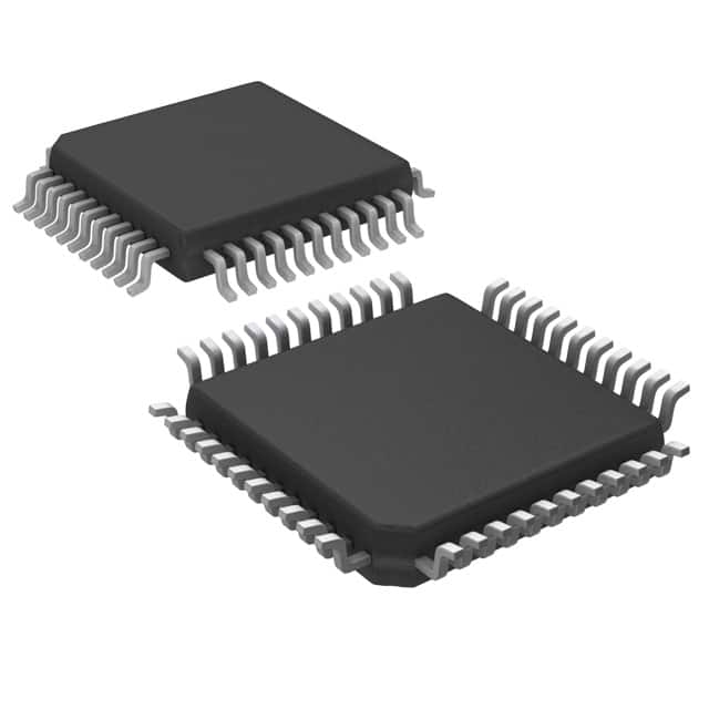
- Part No.:
- TEF6890H/V2,557
- Manufacturer:
- NXP Semiconductors
- Category:
- Audio Special Purpose
- Package:
- 44-QFP
- Datasheet:
-
 TEF6890H/V2,557.pdf
- Description:
- IC AUDIO TONE PROCESSOR 44PQFP
- Quantity:
- Payment:

- Shipping:

Inventory:4,771
Please send an inquiry. Send us your inquiry, and we will respond immediately.
Product details
Overview
TEF6890H/V2,557 from NXP Semiconductors (formerly Philips Semiconductors) is a monolithic BiMOS car radio integrated signal processor for FM/AM stereo decoding, RDS demodulation, and audio tone/volume control. It operates from 8–9 V, integrates I²C-bus interface (400 kHz), delivers 75 dB S/N ratio, supports 50/75 µs de-emphasis selection, and enables real-time weak-signal processing via USN/WAM detectors - deployed in OEM automotive head units.
For engineers reviewing the TEF6890H/V2,557 datasheet, TEF6890H/V2,557 pinout, TEF6890H/V2,557 application, or TEF6890H/V2,557 equivalent, this page provides verified functional context, validated pin roles, confirmed audio path specifications, and manufacturer-confirmed alternative options for automotive infotainment signal chain design.
Technical Context
The TEF6890H/V2,557 implements a dual-path FM/AM signal processing architecture: one MPX path (FMMPX) feeds stereo decoding with PLL-based 38 kHz subcarrier regeneration using external 75.4 kHz reference (from TEA684x tuner), while a second MPX path (MPXRDS) routes to RDS demodulation and noise detection circuits. Its stereo decoder includes pilot cancellation, roll-off correction (4 coarse + 16 fine steps), and dynamic stereo blend (FMSNC) controlled by weak-signal logic.
Weak signal processing uses three parallel digital quality metrics - LEVEL (RF level), USN (ultrasonic noise at MPXRDS output), and WAM (wideband AM on LEVEL signal) - each digitized and processed to drive soft mute, high-cut control (HCC), and stereo blend with programmable attack/decay timing, start thresholds, and slopes. All audio controls (volume, treble, bass, fader) include Audio Step Interpolation (ASI) to eliminate switching pops.
Key Specifications
| Parameter | Value and Actual Design Meaning |
|---|---|
| Supply Voltage | 8.0–9.0 V - matches automotive battery range; requires no external LDO for core operation. |
| Supply Current (Normal Mode) | 28 mA - enables low-power standby modes (15–24 mA) without sacrificing audio fidelity. |
| S/N Ratio | 75 dB (20 Hz–15 kHz) - meets OEM broadcast audio quality requirements for cabin listening. |
| THD | 0.3% max (FM mono) - ensures clean audio output even at full volume without distortion artifacts. |
| I²C-Bus Speed | 400 kHz Fast Mode - supports rapid configuration updates during station search or RDS data acquisition. |
| De-emphasis Selection | 50 µs or 75 µs via I²C - aligns with regional broadcast standards (EU vs. US FM). |
| Volume Control Range | +20 dB to −79 dB in 1 dB steps - covers full dynamic range from quiet cabin to high-noise driving conditions. |
Pinout & Package
TEF6890H/V2,557 is housed in a plastic QFP44 package (SOT307-2), measuring 10 × 10 × 1.75 mm with 1.3 mm lead length - optimized for compact automotive PCB layouts and reflow soldering compatibility.
| Pin/Terminal | Circuit Role | Design Meaning |
|---|---|---|
| FMMPX (Pin 5) | FM multiplex input for stereo decoding | Primary audio path into PLL-based stereo decoder; gain configurable (0–23.5 dB) for tuner interface matching. |
| MPXRDS (Pin 6) | FM multiplex input for RDS/noise detection | Dedicated path to RDS demodulator and FM noise blanker; includes 100 kHz high-pass filter for USN extraction. |
| LEVEL (Pin 1) | Level detector input | Analog voltage representing RF signal strength; used by all weak-signal functions (soft mute, HCC, SNC) and readable via I²C. |
| RDCL / RDDA / RDQ (Pins 39–38–37) | RDS clock, data, and quality outputs | Standard RDS/RBDS interface signals - no external crystal required; synchronized to tuner's 75.4 kHz reference. |
| LFOUT / RFOUT / LROUT / RROUT (Pins 27–28–29–30) | Four-channel audio outputs | Direct-drive capability for front/rear amplifiers; each channel includes independent fader/mute attenuation (0 to −59 dB). |
| NAV (Pin 32) | Navigation voice input | External mono audio injection point; mixed with main audio via internal output mixer for turn-by-turn prompts. |
| SCL / SDA / ADDR (Pins 43–42–44) | I²C-bus interface | Configurable slave address (ADDR); supports gated bus loop-through to tuner ICs to reduce crosstalk and simplify layout. |
Key Features
| Feature | Design Value |
|---|---|
| Integrated RDS/RBDS Demodulator | Eliminates need for external crystal oscillator; uses tuner-provided 75.4 kHz reference - reduces BOM count and board space. |
| Fully Integrated FM/AM Noise Blanker | Sample-and-hold (FM) and muting (AM) architectures suppress ignition noise without external components or microcontroller intervention. |
| Programmable Weak Signal Processing | USN/WAM/LEVEL detectors feed three independent control loops (soft mute, stereo blend, HCC) with user-defined thresholds, slopes, and timing. |
| Audio Step Interpolation (ASI) | Applies smooth logarithmic transitions to volume, treble, bass, fader, and mute - prevents audible clicks during real-time tuning or navigation prompts. |
| Four-Input Selector with NAV Mix | Supports CD, TAPE, PHONE, and AM/FM sources plus overlay of navigation voice (NAV) on any output channel - enables seamless UI-driven audio routing. |
Applications
| Automotive FM/AM Head Unit | OEM Infotainment System |
|---|---|
Use Scenario: Integrated radio module in mid-tier vehicle dashboard delivering broadcast audio, RDS traffic announcements, and navigation voice prompts. IC Role / Device Role / Timing Role: Central signal processor handling stereo decoding, weak-signal adaptation, RDS data recovery, and multi-source audio mixing. Use Value: Enables robust reception in urban multipath environments and rural weak-signal zones while maintaining consistent audio quality across varying supply voltages (8–9 V). |
Use Scenario: Scalable platform supporting multiple vehicle variants with shared hardware, requiring flexible audio routing and firmware-upgradable features. IC Role / Device Role / Timing Role: Configurable audio front-end with I²C-controlled tone/volume, ASI-smoothed transitions, and NAV mixing for human-machine interface compliance. Use Value: Reduces firmware complexity by offloading real-time audio adaptation (soft mute, stereo blend) to dedicated analog/digital logic - improves system responsiveness. |
| Aftermarket Car Stereo | RDS-Enabled Navigation Radio |
Use Scenario: Compact aftermarket unit integrating tuner, DSP, and amplifier driver stages on single PCB. IC Role / Device Role / Timing Role: Single-chip solution replacing discrete op-amps, filters, and logic - handles IF-to-audio conversion, tone shaping, and output drive. Use Value: Cuts component count by >30 vs. legacy designs; QFP44 footprint allows dense layout without thermal derating concerns (Rth(j-a) = 61 K/W). |
Use Scenario: Navigation system that overlays spoken directions onto live FM audio without muting or interrupting broadcast content. IC Role / Device Role / Timing Role: Audio mixer with NAV input and ASI-enabled fade-in/fade-out - synchronizes voice prompts with RDS AF switching events. Use Value: Maintains uninterrupted audio continuity during RDS Alternative Frequency updates via ASI-controlled AF mute - eliminates perceptible dropouts. |
Equivalent & Alternatives
The following parts are listed as comparable options for similar car radio signal processor applications.
| Alternative Part | Technical Difference | Application Difference | Selection Advice |
|---|---|---|---|
| TEF6892H/V2,557 | Same pinout and register map; adds enhanced weather band de-emphasis (15 µs) and extended temperature range (−40°C to +105°C). | Required for vehicles operating in extreme climates or supporting NOAA weather band reception. | Select when wider ambient operating range or weather band support is mandatory; otherwise TEF6890H/V2,557 suffices for standard FM/AM/RDS use. |
| SAF7750HN/V1,557 | Successor generation with integrated ADC/DAC, higher integration (no external coupling caps needed), but requires different I²C initialization sequence and lacks NAV input mixer. | Targets next-gen platforms needing digital audio interface (I²S) and software-defined audio processing. | Choose only if migrating to fully digital signal chain; not drop-in compatible due to missing NAV mixing and altered control protocol. |
Compared with TEF6890H/V2,557, the TEF6892H/V2,557 extends environmental robustness and weather band capability without changing layout or firmware logic, while the SAF7750HN/V1,557 shifts architecture toward digital audio domains - demanding redesign of both hardware interface and control software.
Availability
TEF6890H/V2,557 is available at Aetrix Electronics and suitable for automotive infotainment systems, OEM head unit replacements, and RDS-enabled navigation radios requiring stable component supply, long-lifecycle support, and traceable sourcing.
Supply support for TEF6890H/V2,557 includes scheduled delivery planning, volume procurement assistance, BOM continuity management, traceable sourcing, and lifecycle availability coordination for OEM customers, industrial embedded developers, connected-device designers, and electronics production programs.
Manufacturer
NXP Semiconductors acquired Philips Semiconductors in 2006 and maintains full technical documentation and legacy support for the TEF6890H series - a cornerstone of automotive analog signal processing since 2003.
The TEF6890H/V2,557 belongs to NXP's legacy car radio signal processor family, designed specifically for cost-sensitive, high-reliability analog-dominant infotainment systems where integration, power efficiency, and EMI resilience are critical.
FAQ
What is the function of the MPXRDS pin on the TEF6890H/V2,557?
The MPXRDS pin (Pin 6) carries the FM multiplex signal to the RDS demodulator, FM noise blanker, and ultrasonic noise (USN) detector. It feeds a dedicated 100 kHz high-pass filter to extract USN components and provides the baseband signal for RDS clock/data recovery - distinct from the FMMPX path used for stereo decoding. This separation ensures RDS integrity during weak-signal conditions where stereo decoding may be degraded.
Does the TEF6890H/V2,557 require an external crystal for RDS operation?
No, the TEF6890H/V2,557 does not require an external crystal for RDS operation. It uses the 75.4 kHz reference frequency supplied by compatible tuner ICs (e.g., TEA684x) via the FREF pin (Pin 11). This reference drives both the stereo decoder's auxiliary PLL and the RDS demodulator, eliminating crystal cost, board space, and layout sensitivity - a key design advantage confirmed in Section 1.6 and 7.7 of the datasheet.
How does the Audio Step Interpolation (ASI) feature work in the TEF6890H/V2,557?
ASI in the TEF6890H/V2,557 applies logarithmic interpolation to volume, treble, bass, fader, and mute adjustments - smoothing abrupt gain changes that cause audible pops. Each control transition is divided into 16 steps with programmable duration (4 settings via I²C), ensuring silent switching during navigation prompts or station changes. This function is implemented in analog domain circuitry and requires no host MCU intervention.
Can the TEF6890H/V2,557 process AM and FM signals simultaneously?
The TEF6890H/V2,557 processes AM and FM signals in time-multiplexed mode, not true simultaneity. Its input selector allows only one active source (AM, FM, CD, TAPE, or PHONE) at a time. However, the AM path shares noise blanking and weak-signal logic with FM - e.g., AM soft mute and high-cut control use the same LEVEL detector and I²C-configurable parameters as FM, enabling consistent audio behavior across bands.
What is the maximum input voltage allowed at the NAV pin of the TEF6890H/V2,557?
The NAV pin (Pin 32) accepts a maximum RMS input voltage of 0.3 V at 1 kHz with 1% THD, as specified in the Quick Reference Data table (Page 5). Exceeding this level risks clipping or distortion in the mixed output. The NAV signal is internally summed with main audio channels and routed through the same fader/mute blocks - making it essential to match source impedance and amplitude to avoid imbalance in multi-zone audio distribution.
TEF6890H/V2,557 Specifications
- Product attributes
- Attribute value
- Manufacturer:
- NXP Semiconductors
- Series:
- -
- Package/Case:
- 44-QFP
- Packaging:
- Tray
- Product Status:
- Obsolete
- Function:
- Audio Tone Processor
- Applications:
- Audio
- Number of Channels:
- 6
- Interface:
- I2C
- Voltage - Supply:
- 8V ~ 9V
- Operating Temperature:
- -40°C ~ 85°C (TA)
- Specifications:
- AM, FM
- Mounting Type:
- Surface Mount
- Grade:
- Automotive
TEF6890H/V2,557 FAQ
1.How can I place an order for TEF6890H/V2,557 through Aetrix?
Please submit a Request for Quotation (RFQ) for TEF6890H/V2,557 on Aetrix. Our sales agent will provide a competitive quotation and guide you through the order confirmation once you accept the terms.
2.Are the price and stock information for TEF6890H/V2,557 reliable?
The price and inventory of TEF6890H/V2,557 are updated periodically and may fluctuate due to market conditions. Stock and pricing data are typically refreshed every 24 hours. Quotation validity for TEF6890H/V2,557 is usually 5 days.
3.What payment methods are accepted for TEF6890H/V2,557?
We accept Wire Transfer, PayPal, Credit Card, Western Union, MoneyGram, and Escrow for TEF6890H/V2,557 transactions.
Note: Certain payment methods may incur a processing fee.
4.How is shipping managed for TEF6890H/V2,557?
TEF6890H/V2,557 orders can be shipped via leading logistics carriers, including DHL, UPS, FedEx, TNT, or Registered Mail.
Once your TEF6890H/V2,557 order is processed, you will receive an email with the shipment details and tracking number.
Note: Tracking information may take up to 24 hours to appear. Express delivery typically takes 3–5 business days.
5.How can I obtain technical support or documentation for TEF6890H/V2,557?
For technical support, including TEF6890H/V2,557 datasheets, pinout diagrams, or application guidance, please contact our engineering support team. They can provide detailed documentation and assistance for your TEF6890H/V2,557 requirements.
6.How does Aetrix verify that TEF6890H/V2,557 is sourced from the original manufacturer or authorized distributors?
All TEF6890H/V2,557 products on Aetrix are procured from qualified distributors and authorized channels. Our dedicated quality assurance team conducts strict verification, including traceability checks and, if necessary, third-party testing. This ensures that TEF6890H/V2,557 meets industry standards.
7.What is the process for return or replacement of TEF6890H/V2,557?
All TEF6890H/V2,557 units undergo pre-shipment inspection (PSI). If there is an issue with TEF6890H/V2,557, returns or replacements are accepted under the following conditions:
1.Quantity discrepancies, incorrect items, or visible external defects (such as breakage or corrosion), acknowledged by Aetrix.
2.The issue is reported within 90 days of delivery.
3.The TEF6890H/V2,557 part is unused and in its original packaging.
Return procedure for TEF6890H/V2,557:
1.Submit a request within 90 days.
2.Obtain a Return Material Authorization (RMA) from Aetrix.
TEF6890H/V2,557 Tags

-
SA571DR2G
onsemi
-
ADAU7002ACBZ-R7
Analog Devices Inc.

-
DRV135UA/2K5
Texas Instruments

-
DRV134UA/1K
Texas Instruments

-
DRV134PA
Texas Instruments
-
DRV134UA
Texas Instruments
-
DRV135UA
Texas Instruments
-
SA572DR2G
onsemi
-
PGA2311U/1K
Texas Instruments
-
SI8244BB-D-IS1R
Skyworks Solutions Inc.

-
CS8416K-CZZR
Cirrus Logic Inc.
-
SRC4392IPFBR
Texas Instruments
Tech Hub

A practical engineering guide to 3.3V and 5V logic compatibility, input thresholds, resistor dividers, translator ICs, MOSFET level shifting, I2C pull-ups, timing limits and power-sequencing risks.

The 74HC595 uses push-pull logic outputs, while the TPIC6B595 uses 50 V open-drain DMOS sinks for higher-power loads. This guide compares timing, current limits, 3.3 V interfacing, load wiring, thermal…

The 74HC595 converts serial data into eight stable parallel outputs. This guide covers pin functions, shift and storage timing, OE and MR behavior, drive-current limits, cascading, voltage compatibilit…

A technical comparison of level-sensitive latches and edge-triggered flip-flops, covering timing windows, setup and hold limits, master–slave operation, time borrowing, race-through, HDL inference and…

A D latch stores one bit while Enable controls when data can pass. This reference covers gate-level operation, truth tables, transparency, setup and hold timing, LE versus OE, common ICs and practical …

An SR latch stores one bit through cross-coupled feedback. This engineering reference covers NOR and NAND implementations, truth tables, forbidden-state recovery, gated operation, switch debouncing, fa…

Latch circuits retain one bit through feedback. This technical reference covers SR and D latches, truth tables, transparency, timing limits, latch-versus-flip-flop behavior, applications and common log…

An engineering guide to LED driver operation, constant-current and constant-voltage outputs, linear and switching topologies, dimming, IC selection, calculations, replacement compatibility, and fault c…

Operational amplifier guide covering op amp basics, feedback, ideal vs real op amps, common configurations, buffer circuits, offset, bias current, gain-bandwidth, slew rate, rail-to-rail limits and sel…

Jumper cables guide covering safe connection order, red and black clamp placement, final ground connection, cable gauge, length, clamp quality, copper vs CCA cables, jump starter comparison and battery…


