
 My Inquiry
 My Account


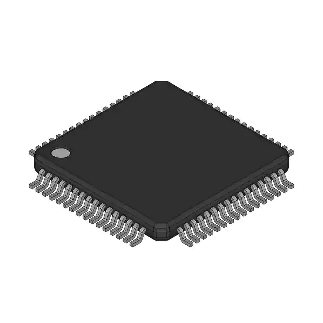
Texas Instruments TFP513PAP
- Part No.:
- TFP513PAP
- Manufacturer:
- Texas Instruments
- Category:
- RF Transmitters
- Package:
- -
- Datasheet:
-
 TFP513PAP.pdf
- Description:
- CONSUMER CIRCUIT, CMOS, PQFP64
- Quantity:
- Payment:

- Shipping:

Inventory:19,813
Please send an inquiry. Send us your inquiry, and we will respond immediately.
Product details
Overview
TFP513PAP from Texas Instruments is a DVI 1.0-compliant digital transmitter IC that encodes and serializes RGB pixel data for transmission over TMDS differential links. It supports VGA-to-UXGA resolutions (25–165 MHz pixel rates), operates on a single 3.3-V supply, integrates embedded HDCP keys, and features dual-edge/24-bit input modes with adjustable 1.1–1.8-V or standard 3.3-V CMOS signal levels - used in PC graphics cards and flat-panel display interfaces.
For engineers reviewing the TFP513PAP datasheet, TFP513PAP pinout, TFP513PAP application, or TFP513PAP equivalent, key selection considerations include TMDS output skew tolerance (≤1.2 ns inter-pair), programmable I²C configuration, hot-plug detection capability, and compatibility with Intel 81x chipset digital video ports.
Technical Context
The TFP513PAP implements a full TMDS encoder with three differential output channels (TX0±, TX1±, TX2±) and a differential clock channel (TXC±), supporting both active-video (RGB) and blanking-interval (HSYNC/VSYNC/CTL) encoding. Its universal graphics controller interface accepts 12-bit dual-edge or 24-bit single-edge pixel buses with configurable VREF-based input voltage thresholds.
It integrates an on-chip PLL with enhanced noise immunity via internal regulators and bypass capacitors, delivers ≤150 ps output clock jitter, and provides data de-skew trimming (350 ps increments) to compensate for input timing misalignment between IDCK± and pixel/control signals.
Key Specifications
| Parameter | Value and Actual Design Meaning |
|---|---|
| Pixel Rate Support | 25 MHz to 165 MHz - enables UXGA (1600×1200@60 Hz) and lower resolutions without external clock synthesis. |
| Input Data Interface | 12-bit dual-edge or 24-bit single-edge - allows glueless connection to diverse graphics controllers including Intel 81x chipsets. |
| Input Signal Levels | Adjustable 1.1–1.8 V or standard 3.3 V CMOS - reduces EMI and enables interoperability with low-voltage GPU I/Os. |
| TMDS Output Swing | 400–600 mVP–P (single-ended) - meets DVI 1.0 electrical compliance with 50-Ω termination. |
| HDCP Compliance | HDCP Rev. 1.0 with embedded preprogrammed keys - eliminates external EEPROM and licensing overhead for secure video transmission. |
| Power Supply | Single 3.3-V supply (DVDD/PVDD/TVDD) - simplifies board power architecture and reduces BOM count. |
| Output Skew | ≤50 ps intra-pair, ≤1.2 ns inter-pair - ensures timing integrity across all four TMDS channels at 165 MHz. |
Pinout & Package
TFP513PAP is housed in a 64-pin TQFP package with TI's PowerPAD™ thermal enhancement, featuring exposed die paddle for improved heat dissipation in high-speed digital applications.
| Pin/Terminal | Circuit Role | Design Meaning |
|---|---|---|
| DATA[23:0] | Parallel pixel/data input bus | Accepts 24-bit RGB data in single-edge mode or upper/lower 12-bit halves in dual-edge mode; unused bits tied to GND/VDD. |
| IDCK+/IDCK− | Differential clock input | Provides timing reference for latching DATA/DE/HSYNC/VSYNC; crossover point used as edge trigger in low-swing mode. |
| TX0±, TX1±, TX2±, TXC± | TMDS differential outputs | Transmit blue/green/red pixel data and sync/control signals during active/blanking intervals; require 50-Ω termination. |
| BSEL/SCL, DSEL/SDA | I²C interface / bus select | Configurable dual-function pins: set input mode (12-/24-bit) when I²C disabled; serve as I²C clock/data when enabled. |
| EDGE/HTPLG | Latch edge select / hot-plug detect | Selects rising/falling edge latching in 24-bit mode; monitors DVI receiver presence when I²C enabled. |
| TFADJ | Full-scale output adjust | Controls TMDS swing amplitude via external pullup resistor (505–515 Ω) to TVDD for DVI-compliant 400–600 mVP–P. |
| MSEN | Monitor sense output | Open-drain indicator of powered-on DVI receiver in dc-coupled systems; programmable via I²C when enabled. |
Key Features
| Feature | Design Value |
|---|---|
| DVI 1.0 & HDCP 1.0 compliance | Fully satisfies industry-standard digital video interface and content protection requirements without external key storage. |
| Programmable I²C interface | Enables runtime reconfiguration of input modes, de-skew trim, HDCP settings, and monitor detection behavior. |
| Universal graphics controller interface | Supports multiple clock/data formats (dual/single-edge, differential/single-ended) to interface seamlessly with legacy and modern GPUs. |
| On-chip regulators & bypass caps | Reduces system-level BOM cost and PCB area by integrating noise-suppression circuitry for PLL stability. |
| Hot-plug and receiver detection | Allows dynamic display enumeration and power management in desktop PCs and docking stations without host intervention. |
| Data de-skew adjustment | 350-ps resolution trimming compensates for PCB trace length mismatches between clock and data paths. |
Applications
| PC Graphics Card Interface | Digital Monitor Input Bridge |
|---|---|
Use Scenario: Integrating DVI output into discrete or integrated GPU designs targeting desktop and workstation markets. IC Role / Device Role / Timing Role: DVI transmitter converting parallel RGB pixel bus and sync signals into serialized TMDS streams for cable transmission. Use Value: Eliminates need for external level-shifting or clock-domain crossing logic due to flexible 1.1–1.8 V input support and dual-edge sampling. |
Use Scenario: Enabling DVI connectivity in LCD monitor mainboards receiving video from external sources. IC Role / Device Role / Timing Role: Final-stage serializer driving TMDS pairs to DVI connector with precise inter-channel skew control. Use Value: Meets strict DVI 1.0 skew and jitter specs (≤1.2 ns inter-pair, ≤150 ps clock jitter) ensuring reliable 165 MHz pixel transmission. |
| Intel 81x Chipset Companion | HDCP-Enabled Media Player |
Use Scenario: Adding compliant DVI output to motherboards based on Intel 810/815/820 series chipsets. IC Role / Device Role / Timing Role: Glueless interface translating Intel DVP-format 12-bit bus into TMDS with no additional logic or buffers. Use Value: Pin- and functional-compatibility with Intel reference design reduces validation time and layout risk. |
Use Scenario: Securing high-definition video output in set-top boxes and Blu-ray players requiring HDCP authentication. IC Role / Device Role / Timing Role: HDCP cipher engine with embedded keys performing real-time encryption of TMDS payload. Use Value: Preprogrammed, encrypted keys eliminate external EEPROM, simplify certification, and prevent key extraction attacks. |
Equivalent & Alternatives
The following parts are listed as comparable options for similar DVI transmitter applications.
| Alternative Part | Technical Difference | Application Difference | Selection Advice |
|---|---|---|---|
| SiI164 | Pin-compatible but lacks embedded HDCP keys; requires external EEPROM for key storage and license procurement. | Suitable for non-HDCP systems or where key management is handled externally; higher BOM cost and security overhead. | Choose SiI164 only if HDCP is not required or customer manages key provisioning independently. |
| TFP514PAP | Successor with identical pinout and enhanced jitter performance (≤100 ps); supports same resolutions and HDCP 1.0. | Drop-in upgrade path for new designs seeking improved signal integrity; not recommended for legacy qualification-critical programs. | Prefer TFP514PAP for new designs requiring tighter timing margins; verify HDCP key compatibility with existing firmware. |
Compared with SiI164, TFP513PAP reduces system cost and security complexity via embedded HDCP keys; compared with TFP514PAP, it offers proven field reliability at slightly relaxed jitter specs - making it optimal for cost-sensitive, volume-manufactured DVI endpoints.
Availability
TFP513PAP is available at Aetrix Electronics and suitable for PC graphics cards, digital monitor interfaces, Intel chipset-based motherboards, and HDCP-enabled media players requiring stable component supply across long production lifecycles.
Supply support for TFP513PAP includes scheduled delivery planning, volume procurement assistance, BOM continuity management, traceable sourcing, and lifecycle availability coordination for OEM customers, industrial embedded developers, connected-device designers, and electronics production programs.
Manufacturer
Texas Instruments is a global semiconductor leader specializing in analog, embedded processing, and digital signal technologies, with decades of experience in display interface solutions.
The TFP513PAP belongs to TI's PanelBus™ family of DVI-compliant transmitters, designed specifically for high-fidelity, low-latency digital video bridging between graphics controllers and flat-panel displays.
FAQ
What is the primary function of the TFP513PAP in a DVI system?
The TFP513PAP serves as a DVI 1.0-compliant digital transmitter that converts parallel RGB pixel data and sync signals into serialized TMDS differential streams for transmission over twisted-pair cables. It performs TMDS encoding, HDCP encryption, and drives four differential output channels (three data, one clock), enabling resolutions up to UXGA at 165 MHz. The TFP513PAP is essential for establishing secure, high-bandwidth digital video links in PC graphics and display systems.
Does the TFP513PAP require external HDCP key storage?
No, the TFP513PAP includes embedded preprogrammed HDCP keys with on-chip encryption, eliminating the need for external EEPROM or flash memory. This integration removes the requirement for customers to procure HDCP licenses separately or implement key management firmware. The TFP513PAP handles key decryption and cipher operations internally, meeting HDCP Revision 1.0 compliance without external components.
How does the TFP513PAP support different graphics controller interfaces?
The TFP513PAP supports both 12-bit dual-edge and 24-bit single-edge input modes via pin-strapping (BSEL) or I²C configuration. It accepts adjustable 1.1–1.8 V or standard 3.3 V CMOS signal levels using the VREF pin, and supports fully differential or single-ended clock inputs (IDCK±). This universal interface enables direct connection to Intel 81x chipsets and other GPU platforms without level shifters or clock buffers - a core capability of the TFP513PAP.
What package type and thermal features does the TFP513PAP use?
The TFP513PAP is packaged in a 64-pin TQFP with TI's PowerPAD™ structure, which incorporates an exposed thermal pad on the underside of the package. This design enhances heat dissipation from the high-speed TMDS drivers and PLL circuitry, improving reliability under sustained 165 MHz operation. The PowerPAD™ requires soldering to a large copper pour on the PCB for optimal thermal performance - a defining mechanical feature of the TFP513PAP.
Can the TFP513PAP be used in hot-plug detection applications?
Yes, the TFP513PAP supports hot-plug detection through the EDGE/HTPLG pin when the I²C interface is enabled (ISEL = high). In this mode, the pin monitors the DVI receiver's hot-plug signal per VESA P&D and DFP standards, requiring only a 1-kΩ series resistor. It also provides monitor sense (MSEN) output to indicate powered-on receiver presence - both functions are integral to the TFP513PAP's role in dynamic display enumeration and power-aware systems.
TFP513PAP Specifications
- Product attributes
- Attribute value
- Manufacturer:
- Texas Instruments
- Series:
- *
- Package/Case:
- -
- Packaging:
- Bulk
- Product Status:
- Active
- Programmable:
- Not Verified
- Frequency:
- -
- Applications:
- -
- Modulation or Protocol:
- -
- Data Rate (Max):
- -
- Power - Output:
- -
- Current - Transmitting:
- -
- Data Interface:
- -
- Antenna Connector:
- -
- Memory Size:
- -
- Features:
- -
- Voltage - Supply:
- -
- Operating Temperature:
- -
- Grade:
- -
- Qualification:
- -
- Mounting Type:
- -
- Supplier Device Package:
- -
TFP513PAP FAQ
1.How can I place an order for TFP513PAP through Aetrix?
Please submit a Request for Quotation (RFQ) for TFP513PAP on Aetrix. Our sales agent will provide a competitive quotation and guide you through the order confirmation once you accept the terms.
2.Are the price and stock information for TFP513PAP reliable?
The price and inventory of TFP513PAP are updated periodically and may fluctuate due to market conditions. Stock and pricing data are typically refreshed every 24 hours. Quotation validity for TFP513PAP is usually 5 days.
3.What payment methods are accepted for TFP513PAP?
We accept Wire Transfer, PayPal, Credit Card, Western Union, MoneyGram, and Escrow for TFP513PAP transactions.
Note: Certain payment methods may incur a processing fee.
4.How is shipping managed for TFP513PAP?
TFP513PAP orders can be shipped via leading logistics carriers, including DHL, UPS, FedEx, TNT, or Registered Mail.
Once your TFP513PAP order is processed, you will receive an email with the shipment details and tracking number.
Note: Tracking information may take up to 24 hours to appear. Express delivery typically takes 3–5 business days.
5.How can I obtain technical support or documentation for TFP513PAP?
For technical support, including TFP513PAP datasheets, pinout diagrams, or application guidance, please contact our engineering support team. They can provide detailed documentation and assistance for your TFP513PAP requirements.
6.How does Aetrix verify that TFP513PAP is sourced from the original manufacturer or authorized distributors?
All TFP513PAP products on Aetrix are procured from qualified distributors and authorized channels. Our dedicated quality assurance team conducts strict verification, including traceability checks and, if necessary, third-party testing. This ensures that TFP513PAP meets industry standards.
7.What is the process for return or replacement of TFP513PAP?
All TFP513PAP units undergo pre-shipment inspection (PSI). If there is an issue with TFP513PAP, returns or replacements are accepted under the following conditions:
1.Quantity discrepancies, incorrect items, or visible external defects (such as breakage or corrosion), acknowledged by Aetrix.
2.The issue is reported within 90 days of delivery.
3.The TFP513PAP part is unused and in its original packaging.
Return procedure for TFP513PAP:
1.Submit a request within 90 days.
2.Obtain a Return Material Authorization (RMA) from Aetrix.
TFP513PAP Tags

-
MICRF113YM6-TR
Microchip Technology
-
PIC12LF1840T39AT-I/ST
Microchip Technology

-
MAX41460GUB+T
Analog Devices Inc./Maxim Integrated
-
SX1230I066TRT
Semtech Corporation
-
SI4010-C2-GS
Silicon Labs
-
CC1070RSQR
Texas Instruments
-
TXM-418-LR
TE Connectivity Linx
-
TXM-433-LR
TE Connectivity Linx
-
TXM-418-KH3
TE Connectivity Linx

-
TX7332ZBX
Texas Instruments
-
MICRF114T-I/OT
Microchip Technology
-
MICRF112YMM-TR
Microchip Technology
Tech Hub

A practical engineering guide to 3.3V and 5V logic compatibility, input thresholds, resistor dividers, translator ICs, MOSFET level shifting, I2C pull-ups, timing limits and power-sequencing risks.

The 74HC595 uses push-pull logic outputs, while the TPIC6B595 uses 50 V open-drain DMOS sinks for higher-power loads. This guide compares timing, current limits, 3.3 V interfacing, load wiring, thermal…

The 74HC595 converts serial data into eight stable parallel outputs. This guide covers pin functions, shift and storage timing, OE and MR behavior, drive-current limits, cascading, voltage compatibilit…

A technical comparison of level-sensitive latches and edge-triggered flip-flops, covering timing windows, setup and hold limits, master–slave operation, time borrowing, race-through, HDL inference and…

A D latch stores one bit while Enable controls when data can pass. This reference covers gate-level operation, truth tables, transparency, setup and hold timing, LE versus OE, common ICs and practical …

An SR latch stores one bit through cross-coupled feedback. This engineering reference covers NOR and NAND implementations, truth tables, forbidden-state recovery, gated operation, switch debouncing, fa…

Latch circuits retain one bit through feedback. This technical reference covers SR and D latches, truth tables, transparency, timing limits, latch-versus-flip-flop behavior, applications and common log…

An engineering guide to LED driver operation, constant-current and constant-voltage outputs, linear and switching topologies, dimming, IC selection, calculations, replacement compatibility, and fault c…

Operational amplifier guide covering op amp basics, feedback, ideal vs real op amps, common configurations, buffer circuits, offset, bias current, gain-bandwidth, slew rate, rail-to-rail limits and sel…

Jumper cables guide covering safe connection order, red and black clamp placement, final ground connection, cable gauge, length, clamp quality, copper vs CCA cables, jump starter comparison and battery…


