
 My Inquiry
 My Account


Texas Instruments TL7726QDG4
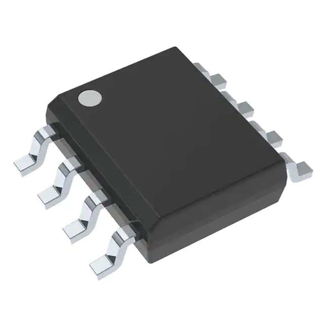
- Part No.:
- TL7726QDG4
- Manufacturer:
- Texas Instruments
- Category:
- Mixed Technology
- Package:
- 8-SOIC (0.154", 3.90mm Width)
- Datasheet:
-
 TL7726QDG4.pdf
- Description:
- TVS DEV MIXED -200/+205V 8SOIC
- Quantity:
- Payment:

- Shipping:

Inventory:2,892
Please send an inquiry. Send us your inquiry, and we will respond immediately.
Product details
Overview
TL7726QDG4 from Texas Instruments is a hex clamping circuit IC designed for transient voltage protection at analog inputs of precision devices. It features six independent clamp channels, ±25 mA sink capability per channel, <10 µA standby current, 0°C to 125°C operating temperature range, and SOIC-8 package - ideal for safeguarding ADCs and microcontrollers in automotive engine control units against large positive/negative transients.
For engineers reviewing the TL7726QDG4 datasheet, TL7726QDG4 pinout, TL7726QDG4 application, or TL7726QDG4 equivalent, key selection criteria include clamping voltage accuracy (±200 mV), latch-up immunity, capacitive load stability, low standby power (<1 mW), and AEC-Q100-relevant thermal robustness across –40°C to 125°C.
Technical Context
The TL7726QDG4 implements six identical voltage-clamp circuits referenced to an internal REF pin, each activating only when input voltage falls below GND or exceeds VREF by ≥200 mV. Each clamp presents high impedance (<10 µA leakage) within the safe band (GND to VREF–50 mV) and switches to low-impedance sink mode (≤25 mA) outside that band.
It operates without output overshoot and maintains stable performance across all capacitive loads - critical for protecting high-impedance analog front-ends. Its settling time is ≤30 µs under ±13 V transient conditions with 600 Ω source impedance, enabling fast response to ESD and load-dump events in industrial and automotive signal chains.
Key Specifications
| Parameter | Value and Actual Design Meaning |
|---|---|
| Clamp Channels | Six independent, identical clamping circuits - enables simultaneous protection of multi-channel ADCs or sensor interfaces. |
| Clamp Current Rating | ±25 mA per channel - sufficient to shunt transient energy without latch-up in CMOS inputs. |
| Clamp Voltage Accuracy | +200 mV above VREF / –200 mV below GND - defines precise overvoltage/undervoltage trip thresholds. |
| Standby Current | <10 µA per channel - minimizes loading on protected signal sources during normal operation. |
| Operating Temperature | –40°C to +125°C - qualified for under-hood automotive and harsh industrial environments. |
| Supply Independence | No VCC required - operates passively using only REF and signal path - eliminates dependency on system power rails. |
| Capacitive Load Stability | Stable for all values - allows direct connection to high-C sensor outputs or long PCB traces without oscillation. |
Pinout & Package
TL7726QDG4 is housed in an 8-pin SOIC (D) package with 1.27 mm pitch, 3.91 mm width, and 1.75 mm max height - compatible with standard surface-mount assembly processes and IPC-7351 land patterns.
| Pin/Terminal | Circuit Role | Design Meaning |
|---|---|---|
| 1 (GND) | Ground reference | Common return for all six clamp circuits; must be low-impedance to handle peak 25 mA sink currents. |
| 2–7 (CLAMP 1–6) | Input/output clamp terminals | Each connects directly to a protected signal line; sinks current when VI < GND or VI > VREF. |
| 8 (REF) | Reference voltage input | External 4.5–5.5 V reference sets clamping threshold; determines VIK+ and VIK– trip points. |
Key Features
| Feature | Design Value |
|---|---|
| Latch-up protection | Prevents CMOS device failure by diverting transient current before silicon parasitic SCR triggers. |
| No output overshoot | Eliminates post-transient ringing that could falsely trigger downstream comparators or ADC sampling. |
| Sub-1 mW standby dissipation | Enables always-on protection in battery-backed or low-power systems without measurable impact on quiescent current. |
| Transient response time ≤30 µs | Meets ISO 7637-2 Pulse 1/2/5a timing requirements for automotive electronics protection. |
| Capacitive load immunity | Supports direct interface to piezoelectric sensors, thermocouple amplifiers, and long analog traces without compensation. |
Applications
| Automotive Engine Control Unit (ECU) Analog Inputs | Industrial PLC Analog Input Modules |
|---|---|
Use Scenario: Protecting 12-bit SAR ADC inputs from alternator load dump (±60 V) and ignition coil flyback spikes in diesel ECU designs. IC Role / Device Role / Timing Role: Passive clamping element placed between sensor harness and ADC input buffer - no timing or clock involvement. Use Value: Prevents permanent damage to ADC input ESD structures while maintaining <10 µA bias current integrity during normal 0–5 V sensor operation. |
Use Scenario: Safeguarding 4–20 mA current loop receiver inputs in factory-floor PLC modules exposed to relay switching transients. IC Role / Device Role / Timing Role: Signal-line clamp positioned ahead of op-amp I/V converter - operates independently of system clock or data rate. Use Value: Enables reliable 24 VDC field-side interfacing without requiring external TVS diodes or complex RC filtering networks. |
| Medical Patient Monitoring Front-Ends | Avionics Sensor Signal Conditioning |
Use Scenario: Shielding ECG/EEG amplifier inputs from electrostatic discharge during patient handling in portable monitors. IC Role / Device Role / Timing Role: First-stage analog protection device - clamps transients before programmable-gain amplifier (PGA) stage. Use Value: Maintains sub-µV input offset stability and preserves common-mode rejection ratio (CMRR) by avoiding nonlinear TVS conduction. |
Use Scenario: Protecting RTD and thermocouple inputs in flight control sensor units subjected to lightning-induced surges per DO-160 Section 22. IC Role / Device Role / Timing Role: Passive overvoltage limiter on analog sensor lines - no power supply or control logic required. Use Value: Provides predictable ±200 mV clamping window referenced to stable 5 V rail - supports deterministic fault analysis for DO-254 compliance. |
Equivalent & Alternatives
The following parts are listed as comparable options for similar clamping circuit applications.
| Alternative Part | Technical Difference | Application Difference | Selection Advice |
|---|---|---|---|
| TL7726IDR | Same circuit architecture and pinout; rated for –40°C to +85°C instead of +125°C. | Limited to under-dash automotive or commercial industrial use; not qualified for engine compartment deployment. | Select TL7726IDR only if ambient temperature remains ≤85°C and cost sensitivity outweighs extended thermal margin. |
| TPD2E001DRYR | Single-channel, dual-diode ESD protector with 15 kV HBM rating; lacks adjustable reference and active clamp behavior. | Designed for board-level ESD only - cannot replace TL7726QDG4 in precision overvoltage/undervoltage clamping roles. | Use TPD2E001DRYR as supplemental ESD layer, not as functional replacement; requires separate VREF and current-sink design. |
Compared with TL7726IDR, TL7726QDG4 delivers guaranteed operation up to 125°C for engine bay placement, while TPD2E001DRYR offers higher ESD immunity but no programmable clamping threshold or multi-channel integration - making TL7726QDG4 uniquely suited for precision analog transient suppression where thermal margin and channel density are critical.
Availability
TL7726QDG4 is available at Aetrix Electronics and suitable for automotive engine control units, industrial PLC analog input modules, medical patient monitoring front-ends, and avionics sensor signal conditioning requiring stable component supply across extended temperature ranges and long production lifecycles.
Supply support for TL7726QDG4 includes scheduled delivery planning, volume procurement assistance, BOM continuity management, traceable sourcing, and lifecycle availability coordination for OEM customers, industrial embedded developers, connected-device designers, and electronics production programs.
Manufacturer
Texas Instruments is a global semiconductor leader specializing in analog, embedded processing, and power management technologies, with decades of automotive-grade reliability validation.
The TL7726QDG4 belongs to TI's legacy precision analog protection portfolio, engineered specifically for high-reliability transient suppression in safety-critical analog signal paths - emphasizing latch-up immunity, thermal robustness, and passive operation without external power.
FAQ
What is the maximum reference voltage supported by TL7726QDG4?
The TL7726QDG4 supports a reference voltage (VREF) range of 4.5 V to 5.5 V per the recommended operating conditions. Exceeding 6 V violates absolute maximum ratings and risks permanent damage. The clamping thresholds scale directly with VREF: VIK+ = VREF + 200 mV and VIK– = –200 mV, so precise 5.0 V regulation is advised for consistent ±200 mV windows. TL7726QDG4 does not regulate VREF internally - it must be supplied externally with low noise and adequate current capability.
Does TL7726QDG4 require a power supply to operate?
No, TL7726QDG4 operates passively and requires no VCC connection. It draws less than 10 µA from the protected signal line in standby and sinks transient current directly to GND through its internal clamp structure. This eliminates dependencies on system power sequencing, reduces BOM count, and ensures protection remains active even during brown-out or power-down states - a key advantage over active protection ICs. TL7726QDG4 functionality is fully defined by the REF voltage and signal path alone.
Can TL7726QDG4 be used with capacitive loads such as piezoelectric sensors?
Yes, TL7726QDG4 is explicitly characterized for stable operation with all values of capacitive load - including high-C piezoelectric transducers and long PCB traces - without oscillation or overshoot. Its internal architecture avoids phase inversion or gain peaking that plagues op-amp-based clamp solutions. When used with piezo sensors, TL7726QDG4 preserves signal fidelity during transient events while adding negligible loading in the 0–5 V operating band. This behavior is confirmed in the datasheet's "Stable Operation for All Values of Capacitive Load" specification.
What is the clamping response time of TL7726QDG4 under a 13 V transient?
Under a ±13 V transient with 600 Ω source impedance and rise time <1 µs, TL7726QDG4 achieves full clamping stabilization in ≤30 µs, measured from 10% to 90% of final clamped voltage (VIK+ or VIK–). This settling time is verified in Figure 1 of the SLAS078C datasheet and meets ISO 7637-2 Pulse 5a surge test requirements for automotive electronics. TL7726QDG4's response is limited only by external RC time constants - the device itself introduces no propagation delay or latency.
Is TL7726QDG4 pin-compatible with other variants like TL7726CD or TL7726ID?
Yes, TL7726QDG4 shares identical SOIC-8 (D) package dimensions, pinout, and electrical interface with TL7726CD and TL7726ID - all have GND on Pin 1, CLAMP1–6 on Pins 2–7, and REF on Pin 8. However, thermal qualification differs: TL7726QDG4 is rated for –40°C to +125°C, while TL7726CD is 0°C to +70°C and TL7726ID is –40°C to +85°C. TL7726QDG4 can be used as a drop-in replacement in existing layouts where extended temperature operation is needed, provided REF voltage and layout thermal management support the higher junction temperature.
TL7726QDG4 Specifications
- Product attributes
- Attribute value
- Manufacturer:
- Texas Instruments
- Package/Case:
- 8-SOIC (0.154", 3.90mm Width)
- Series:
- -
- Packaging:
- Bulk
- Product Status:
- Discontinued at Digi-Key
- Voltage - Clamping:
- -200/+205V
- Technology:
- Mixed Technology
- Number of Circuits:
- 6
- Applications:
- General Purpose
- Grade:
- -
- Qualification:
- -
- Mounting Type:
- Surface Mount
- Supplier Device Package:
- 8-SOIC
TL7726QDG4 FAQ
1.How can I place an order for TL7726QDG4 through Aetrix?
Please submit a Request for Quotation (RFQ) for TL7726QDG4 on Aetrix. Our sales agent will provide a competitive quotation and guide you through the order confirmation once you accept the terms.
2.Are the price and stock information for TL7726QDG4 reliable?
The price and inventory of TL7726QDG4 are updated periodically and may fluctuate due to market conditions. Stock and pricing data are typically refreshed every 24 hours. Quotation validity for TL7726QDG4 is usually 5 days.
3.What payment methods are accepted for TL7726QDG4?
We accept Wire Transfer, PayPal, Credit Card, Western Union, MoneyGram, and Escrow for TL7726QDG4 transactions.
Note: Certain payment methods may incur a processing fee.
4.How is shipping managed for TL7726QDG4?
TL7726QDG4 orders can be shipped via leading logistics carriers, including DHL, UPS, FedEx, TNT, or Registered Mail.
Once your TL7726QDG4 order is processed, you will receive an email with the shipment details and tracking number.
Note: Tracking information may take up to 24 hours to appear. Express delivery typically takes 3–5 business days.
5.How can I obtain technical support or documentation for TL7726QDG4?
For technical support, including TL7726QDG4 datasheets, pinout diagrams, or application guidance, please contact our engineering support team. They can provide detailed documentation and assistance for your TL7726QDG4 requirements.
6.How does Aetrix verify that TL7726QDG4 is sourced from the original manufacturer or authorized distributors?
All TL7726QDG4 products on Aetrix are procured from qualified distributors and authorized channels. Our dedicated quality assurance team conducts strict verification, including traceability checks and, if necessary, third-party testing. This ensures that TL7726QDG4 meets industry standards.
7.What is the process for return or replacement of TL7726QDG4?
All TL7726QDG4 units undergo pre-shipment inspection (PSI). If there is an issue with TL7726QDG4, returns or replacements are accepted under the following conditions:
1.Quantity discrepancies, incorrect items, or visible external defects (such as breakage or corrosion), acknowledged by Aetrix.
2.The issue is reported within 90 days of delivery.
3.The TL7726QDG4 part is unused and in its original packaging.
Return procedure for TL7726QDG4:
1.Submit a request within 90 days.
2.Obtain a Return Material Authorization (RMA) from Aetrix.
TL7726QDG4 Tags
-
ESD03A5V5R17V
Stackpole Electronics Inc
-
ESDU02A5V5R17V
Stackpole Electronics Inc
-
0603ESDA-MLP7
Eaton - Electronics Division
.jpg)
-
0603ESDA2-TR2
Eaton - Electronics Division
-
PS04LTVA1
Eaton - Electronics Division
.jpg)
-
0402ESDA-MLP1
Eaton - Electronics Division
.jpg)
-
0402ESDA-MLP7
Eaton - Electronics Division
-
TPD2S017DBVR
Texas Instruments
.jpg)
-
V2F105A150Y2EDP
KYOCERA AVX
-
82307050029
Würth Elektronik
-
NCP360SNT1G
onsemi
-
V2F118A400Y2EDP
KYOCERA AVX
Tech Hub

A practical engineering guide to 3.3V and 5V logic compatibility, input thresholds, resistor dividers, translator ICs, MOSFET level shifting, I2C pull-ups, timing limits and power-sequencing risks.

The 74HC595 uses push-pull logic outputs, while the TPIC6B595 uses 50 V open-drain DMOS sinks for higher-power loads. This guide compares timing, current limits, 3.3 V interfacing, load wiring, thermal…

The 74HC595 converts serial data into eight stable parallel outputs. This guide covers pin functions, shift and storage timing, OE and MR behavior, drive-current limits, cascading, voltage compatibilit…

A technical comparison of level-sensitive latches and edge-triggered flip-flops, covering timing windows, setup and hold limits, master–slave operation, time borrowing, race-through, HDL inference and…

A D latch stores one bit while Enable controls when data can pass. This reference covers gate-level operation, truth tables, transparency, setup and hold timing, LE versus OE, common ICs and practical …

An SR latch stores one bit through cross-coupled feedback. This engineering reference covers NOR and NAND implementations, truth tables, forbidden-state recovery, gated operation, switch debouncing, fa…

Latch circuits retain one bit through feedback. This technical reference covers SR and D latches, truth tables, transparency, timing limits, latch-versus-flip-flop behavior, applications and common log…

An engineering guide to LED driver operation, constant-current and constant-voltage outputs, linear and switching topologies, dimming, IC selection, calculations, replacement compatibility, and fault c…

Operational amplifier guide covering op amp basics, feedback, ideal vs real op amps, common configurations, buffer circuits, offset, bias current, gain-bandwidth, slew rate, rail-to-rail limits and sel…

Jumper cables guide covering safe connection order, red and black clamp placement, final ground connection, cable gauge, length, clamp quality, copper vs CCA cables, jump starter comparison and battery…


