
 My Inquiry
 My Account


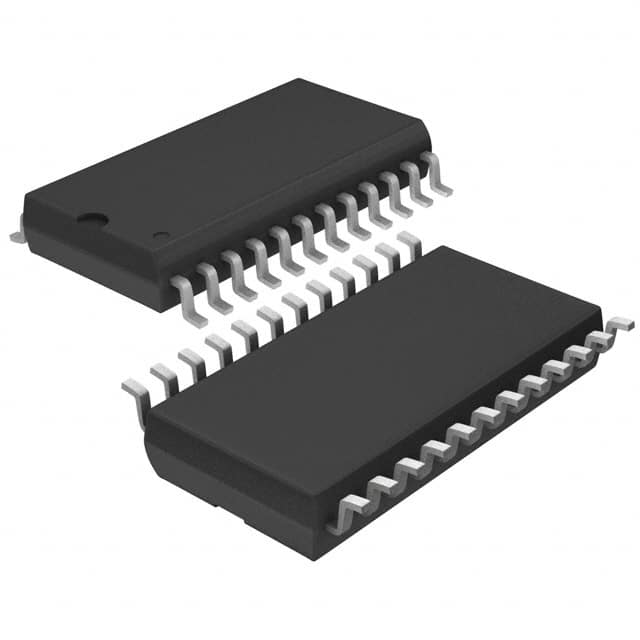
Texas Instruments TLC3578IDWG4
- Part No.:
- TLC3578IDWG4
- Manufacturer:
- Texas Instruments
- Category:
- Analog to Digital Converters (ADC)
- Package:
- 24-SOIC (0.295", 7.50mm Width)
- Datasheet:
-
 TLC3578IDWG4.pdf
- Description:
- IC ADC 14BIT SAR 24SOIC
- Quantity:
- Payment:

- Shipping:

Inventory:3,644
Please send an inquiry. Send us your inquiry, and we will respond immediately.
Product details
Overview
TLC3578IDWG4 from Texas Instruments is a 14-bit, 8-channel single-ended SAR analog-to-digital converter (ADC) with SPI/DSP-compatible serial interface, ±10 V bipolar input range, 200-KSPS maximum throughput, and integrated 8× FIFO. It operates from a single 5-V analog supply and 3-/5-V digital supply, targeting precision data acquisition in industrial process control systems.
For engineers reviewing the TLC3578IDWG4 datasheet, TLC3578IDWG4 pinout, TLC3578IDWG4 application, or TLC3578IDWG4 equivalent, key selection criteria include its 14-bit resolution with ±1 LSB INL, hardware-configurable sampling via CSTART, built-in conversion clock (6.5 MHz internal OSC), and TSSOP-24 package compatibility with industrial temperature range (−40°C to 85°C).
Technical Context
The TLC3578IDWG4 integrates an 8-channel analog multiplexer, sample-and-hold, successive approximation register (SAR), internal 6.5-MHz oscillator, and 8-deep FIFO - enabling autonomous channel sweep and repeat without host intervention. Its dual-mode sampling supports normal (12/44 SCLK) or extended (CSTART-triggered) acquisition for high-impedance sources.
It supports both SPI (CS/SDI/SDO/SCLK) and DSP (FS/SDI/SDO/SCLK) serial protocols, with CS acting as slave select and FS as frame sync. The device features programmable autochannel sweep, hardware default configuration (via SDI tied to DVDD), and bipolar signal scaling with REFP/REFM reference inputs.
Key Specifications
| Parameter | Value and Actual Design Meaning |
|---|---|
| Resolution | 14-bit SAR architecture delivering 16,384 discrete output codes for high-fidelity signal digitization. |
| Throughput Rate | 200 KSPS maximum - enables real-time monitoring of fast transients in motor control or power quality analyzers. |
| Analog Input Range | ±10 V bipolar full-scale range - supports direct connection to industrial sensors and transducers without external level-shifting. |
| INL / DNL | ±1 LSB integral linearity error and ±0.5 LSB differential linearity error - ensures monotonicity and minimal code-width variation across full scale. |
| Power Consumption | 5.8 mA typical in normal operation; 20 µA in power-down mode - suitable for battery-backed or energy-conscious embedded systems. |
| Sampling Flexibility | Hardware-controlled CSTART pin extends sampling period independently of SCLK - critical for accurate digitization of high-source-impedance signals (>25 Ω). |
| Reference Interface | Dedicated REFP and REFM pins support external 4-V reference with 10 µF + 0.1 µF decoupling - stabilizes conversion accuracy against supply noise. |
Pinout & Package
Package: 24-pin TSSOP (DW), RoHS-compliant, body size 7.8 mm × 4.4 mm, 0.65 mm pitch.
| Pin/Terminal | Circuit Role | Design Meaning |
|---|---|---|
| A0–A7 | Analog input channels | 8 single-ended analog inputs; source impedance ≤25 Ω required for normal sampling; CSTART extends hold time for higher impedances. |
| AGND (pins 14, 18) | Analog ground return | Separate low-noise ground reference for analog circuitry; must be isolated from DGND to minimize digital coupling. |
| AVDD (pins 13, 19) | Analog supply | 5-V ±5% regulated analog supply; powers MUX, S/H, SAR, and reference buffer - requires local 10 µF + 0.1 µF decoupling. |
| COMP (pin 17) | Internal compensation | Connect 0.1 µF capacitor to AGND to stabilize internal op-amp loop - mandatory for specified AC performance. |
| CSTART (pin 20) | External sampling trigger | Asynchronous start-of-sampling control; low pulse width determines acquisition time - bypasses SCLK timing constraints. |
| CS (pin 8) | Chip select | Active-low SPI slave select; falling edge resets 4-bit counter and enables serial interface - can be tied to DGND for single-device systems. |
| DGND (pin 6) | Digital ground return | Return path for digital I/O and logic; must connect to system digital ground plane with short, low-inductance trace. |
| DVDD (pin 7) | Digital supply | 3-V to 5-V digital supply; powers serial interface and control logic - decouple with 0.1 µF ceramic capacitor near pin. |
| EOC/INT (pin 4) | End-of-conversion indicator | Open-drain output signaling data readiness; functions as EOC (mode 00) or INT (falling-edge interrupt) - cleared by CS↓, FS↑, or CSTART↓. |
| FS (pin 2) | Frame sync input | DSP interface synchronization signal; rising edge initiates serial frame - tie to DVDD if unused in SPI configurations. |
| REFM (pin 16) | Negative reference input | Connect directly to AGND; establishes lower rail of ±10 V input range - forms reference pair with REFP. |
| REFP (pin 15) | Positive reference input | Accepts 3.96–4.04 V reference voltage; defines upper rail of ±10 V range - requires 10 µF + 0.1 µF decoupling to REFM. |
| SCLK (pin 1) | Serial clock input | Up to 25-MHz clock for SPI/DSP interface; also serves as external conversion clock when selected - disabled during CS high. |
| SDI (pin 3) | Serial data input | Command and configuration interface; first 4 bits decode as ID[15:12]; tie to DVDD for hardware-default initialization. |
| SDO (pin 5) | Serial data output | 3-state MSB-first output of 14-bit conversion result; enters high-Z state after 16th SCLK falling edge or when CS is high. |
Key Features
| Feature | Design Value |
|---|---|
| Built-in 8× FIFO | Enables burst-mode acquisition without host CPU overhead - ideal for oscilloscope-like capture or triggered event logging. |
| Programmable Autochannel Sweep | Automatically sequences through up to 8 analog inputs with configurable repeat - reduces firmware complexity in multi-sensor monitoring. |
| Hardware Default Configuration | Power-on initialization without software setup when SDI is tied to DVDD - accelerates system boot and simplifies design validation. |
| Pseudodifferential Input Support | Allows simultaneous sampling of adjacent channels with common-mode rejection - improves noise immunity in noisy industrial environments. |
| Low-Power Autopower-Down Mode | Reduces current to 175–230 µA during idle periods - extends operational life in portable test equipment and remote sensor nodes. |
Applications
| Industrial Process Control | Motor Drive Current Sensing |
|---|---|
Use Scenario: Continuous monitoring of temperature, pressure, and flow sensors in PLC-based automation systems. IC Role / Device Role / Timing Role: High-accuracy front-end ADC digitizing ±10 V sensor outputs with synchronized sampling across multiple channels. Use Value: 14-bit resolution and ±1 LSB INL ensure precise closed-loop control of actuators and valves within 0.006% full-scale error. |
Use Scenario: Real-time phase current measurement in 3-phase inverter drives using shunt resistors. IC Role / Device Role / Timing Role: Simultaneous sampling of three current feedback paths with hardware-triggered CSTART to eliminate timing skew. Use Value: Extended sampling via CSTART accommodates shunt amplifier settling time, maintaining <0.1% gain error at 200 KSPS. |
| Power Quality Analyzers | Test & Measurement Equipment |
Use Scenario: Digitizing AC voltage and current waveforms for harmonic distortion analysis per IEEE 519. IC Role / Device Role / Timing Role: Bipolar ±10 V input interface capturing true RMS, THD, and SFDR metrics with 79 dB SINAD at 20 kHz. Use Value: 79 dB SINAD and −82 dB THD enable Class A power analyzer compliance with IEC 61000-4-30 Ed. 3. |
Use Scenario: Embedded digitizer module in handheld multimeters and portable oscilloscopes. IC Role / Device Role / Timing Role: Low-power, self-contained ADC subsystem with integrated FIFO and hardware sweep for rapid waveform capture. Use Value: 20 µA power-down current and 5.8 mA active current allow >10-hour battery life while maintaining 14-bit fidelity. |
Equivalent & Alternatives
The following parts are listed as comparable options for similar high-resolution SAR ADC applications.
| Alternative Part | Technical Difference | Application Difference | Selection Advice |
|---|---|---|---|
| ADS8688IPWR | 16-bit resolution, 500-KSPS, integrated PGA and reference; requires external power sequencing. | Higher precision but larger footprint and higher cost; suited for metrology-grade instruments. | Select ADS8688IPWR when 16-bit ENOB and on-chip PGA are required; TLC3578IDWG4 remains optimal for cost-sensitive 14-bit industrial DAQ. |
| MAX11131ETL+ | 14-bit, 500-KSPS, SPI-only interface, no CSTART or FIFO; 2.7–3.6 V digital supply only. | Lacks hardware-triggered sampling and autonomous channel sweep - increases host CPU load in multi-channel systems. | Choose MAX11131ETL+ for ultra-low-voltage portable designs; TLC3578IDWG4 better fits industrial 5-V systems needing flexible timing control. |
Compared with ADS8688IPWR and MAX11131ETL+, the TLC3578IDWG4 uniquely balances 14-bit accuracy, 200-KSPS throughput, hardware-configurable sampling, and integrated FIFO in a compact TSSOP-24 package - making it the preferred choice for deterministic, low-overhead industrial data acquisition where ±10 V bipolar range and −40°C to 85°C operation are essential.
Availability
TLC3578IDWG4 is available at Aetrix Electronics and suitable for industrial process control, motor drive current sensing, power quality analyzers, and portable test equipment requiring stable component supply across extended temperature ranges and long production lifecycles.
Supply support for TLC3578IDWG4 includes scheduled delivery planning, volume procurement assistance, BOM continuity management, traceable sourcing, and lifecycle availability coordination for OEM customers, industrial embedded developers, connected-device designers, and electronics production programs.
Manufacturer
Texas Instruments is a global semiconductor leader specializing in analog and embedded processing technologies, with decades of expertise in precision data converters and industrial-grade ICs.
The TLC3578IDWG4 belongs to TI's high-performance SAR ADC product line, engineered specifically for industrial data acquisition systems demanding robust bipolar input handling, deterministic timing control, and low-power operation in harsh environments.
FAQ
What is the operating temperature range for the TLC3578IDWG4?
The TLC3578IDWG4 is rated for operation from −40°C to +85°C ambient temperature, meeting industrial-grade reliability requirements. This range is validated across all electrical specifications including INL, SINAD, and power consumption - ensuring consistent 14-bit performance in factory-floor or outdoor-mounted equipment where thermal cycling occurs.
Does the TLC3578IDWG4 require an external reference voltage?
Yes, the TLC3578IDWG4 requires external reference connections at REFP and REFM pins. The datasheet specifies a nominal 4-V reference (3.96–4.04 V) applied between REFP and REFM to establish the ±10 V full-scale input range. Decoupling with 10 µF + 0.1 µF capacitors between these pins is mandatory to maintain specified 79 dB SINAD and ±1 LSB INL performance.
How does the CSTART pin function in the TLC3578IDWG4?
The CSTART pin on the TLC3578IDWG4 provides hardware-controlled asynchronous sampling initiation. A high-to-low transition starts analog acquisition; a low-to-high transition places the sample-and-hold into hold mode and begins conversion. Its low-time directly sets sampling duration - enabling accurate digitization of signals from high-impedance sources beyond the 25-Ω limit for normal SCLK-driven sampling.
Can the TLC3578IDWG4 operate with a 3-V digital supply?
Yes, the TLC3578IDWG4 supports digital supply voltages from 2.7 V to 5.5 V on DVDD, making it compatible with 3-V microcontroller interfaces. Digital input thresholds scale accordingly (VIH = 2.1 V min at DVDD = 3 V), and output drive strength is maintained - allowing seamless integration into mixed-supply systems without level shifters.
What is the purpose of the COMP pin on the TLC3578IDWG4?
The COMP pin on the TLC3578IDWG4 is an internal op-amp compensation node requiring a 0.1 µF capacitor connected to AGND. This capacitor stabilizes the reference buffer and analog front-end, preventing oscillation and ensuring specified AC performance - including 79 dB SINAD and −82 dB THD - is achieved across the full operating temperature range.
TLC3578IDWG4 Specifications
- Product attributes
- Attribute value
- Manufacturer:
- Texas Instruments
- Series:
- -
- Package/Case:
- 24-SOIC (0.295", 7.50mm Width)
- Packaging:
- Tube
- Product Status:
- Obsolete
- Number of Bits:
- 14
- Sampling Rate (Per Second):
- 200k
- Number of Inputs:
- 4, 8
- Input Type:
- Pseudo-Differential, Single Ended
- Data Interface:
- SPI
- Configuration:
- MUX-S/H-ADC
- Ratio - S/H:ADC:
- 1:1
- Number of A/D Converters:
- 1
- Architecture:
- SAR
- Reference Type:
- External
- Voltage - Supply, Analog:
- 5V
- Voltage - Supply, Digital:
- 2.7V ~ 5.5V
- Features:
- -
- Operating Temperature:
- -40°C ~ 85°C
- Supplier Device Package:
- 24-SOIC
- Mounting Type:
- Surface Mount
- Grade:
- -
- Qualification:
- -
TLC3578IDWG4 FAQ
1.How can I place an order for TLC3578IDWG4 through Aetrix?
Please submit a Request for Quotation (RFQ) for TLC3578IDWG4 on Aetrix. Our sales agent will provide a competitive quotation and guide you through the order confirmation once you accept the terms.
2.Are the price and stock information for TLC3578IDWG4 reliable?
The price and inventory of TLC3578IDWG4 are updated periodically and may fluctuate due to market conditions. Stock and pricing data are typically refreshed every 24 hours. Quotation validity for TLC3578IDWG4 is usually 5 days.
3.What payment methods are accepted for TLC3578IDWG4?
We accept Wire Transfer, PayPal, Credit Card, Western Union, MoneyGram, and Escrow for TLC3578IDWG4 transactions.
Note: Certain payment methods may incur a processing fee.
4.How is shipping managed for TLC3578IDWG4?
TLC3578IDWG4 orders can be shipped via leading logistics carriers, including DHL, UPS, FedEx, TNT, or Registered Mail.
Once your TLC3578IDWG4 order is processed, you will receive an email with the shipment details and tracking number.
Note: Tracking information may take up to 24 hours to appear. Express delivery typically takes 3–5 business days.
5.How can I obtain technical support or documentation for TLC3578IDWG4?
For technical support, including TLC3578IDWG4 datasheets, pinout diagrams, or application guidance, please contact our engineering support team. They can provide detailed documentation and assistance for your TLC3578IDWG4 requirements.
6.How does Aetrix verify that TLC3578IDWG4 is sourced from the original manufacturer or authorized distributors?
All TLC3578IDWG4 products on Aetrix are procured from qualified distributors and authorized channels. Our dedicated quality assurance team conducts strict verification, including traceability checks and, if necessary, third-party testing. This ensures that TLC3578IDWG4 meets industry standards.
7.What is the process for return or replacement of TLC3578IDWG4?
All TLC3578IDWG4 units undergo pre-shipment inspection (PSI). If there is an issue with TLC3578IDWG4, returns or replacements are accepted under the following conditions:
1.Quantity discrepancies, incorrect items, or visible external defects (such as breakage or corrosion), acknowledged by Aetrix.
2.The issue is reported within 90 days of delivery.
3.The TLC3578IDWG4 part is unused and in its original packaging.
Return procedure for TLC3578IDWG4:
1.Submit a request within 90 days.
2.Obtain a Return Material Authorization (RMA) from Aetrix.
TLC3578IDWG4 Tags
-
ADC081C021CIMKX/NOPB
Texas Instruments

-
MCP3021A5T-E/OT
Microchip Technology
-
TLA2024IRUGR
Texas Instruments
-
MCP3221A5T-E/OT
Microchip Technology
-
MCP3221A5T-I/OT
Microchip Technology
-
MCP3221A4T-E/OT
Microchip Technology
-
MCP3221A6T-E/OT
Microchip Technology
-
MCP3221A0T-E/OT
Microchip Technology
-
MCP3221A1T-E/OT
Microchip Technology

-
ADC121S021CIMFX/NOPB
Texas Instruments

-
MCP3001-I/MS
Microchip Technology

-
MCP3001-I/SN
Microchip Technology
Tech Hub

A practical engineering guide to 3.3V and 5V logic compatibility, input thresholds, resistor dividers, translator ICs, MOSFET level shifting, I2C pull-ups, timing limits and power-sequencing risks.

The 74HC595 uses push-pull logic outputs, while the TPIC6B595 uses 50 V open-drain DMOS sinks for higher-power loads. This guide compares timing, current limits, 3.3 V interfacing, load wiring, thermal…

The 74HC595 converts serial data into eight stable parallel outputs. This guide covers pin functions, shift and storage timing, OE and MR behavior, drive-current limits, cascading, voltage compatibilit…

A technical comparison of level-sensitive latches and edge-triggered flip-flops, covering timing windows, setup and hold limits, master–slave operation, time borrowing, race-through, HDL inference and…

A D latch stores one bit while Enable controls when data can pass. This reference covers gate-level operation, truth tables, transparency, setup and hold timing, LE versus OE, common ICs and practical …

An SR latch stores one bit through cross-coupled feedback. This engineering reference covers NOR and NAND implementations, truth tables, forbidden-state recovery, gated operation, switch debouncing, fa…

Latch circuits retain one bit through feedback. This technical reference covers SR and D latches, truth tables, transparency, timing limits, latch-versus-flip-flop behavior, applications and common log…

An engineering guide to LED driver operation, constant-current and constant-voltage outputs, linear and switching topologies, dimming, IC selection, calculations, replacement compatibility, and fault c…

Operational amplifier guide covering op amp basics, feedback, ideal vs real op amps, common configurations, buffer circuits, offset, bias current, gain-bandwidth, slew rate, rail-to-rail limits and sel…

Jumper cables guide covering safe connection order, red and black clamp placement, final ground connection, cable gauge, length, clamp quality, copper vs CCA cables, jump starter comparison and battery…


