
 My Inquiry
 My Account


Texas Instruments TLC5949DBQR
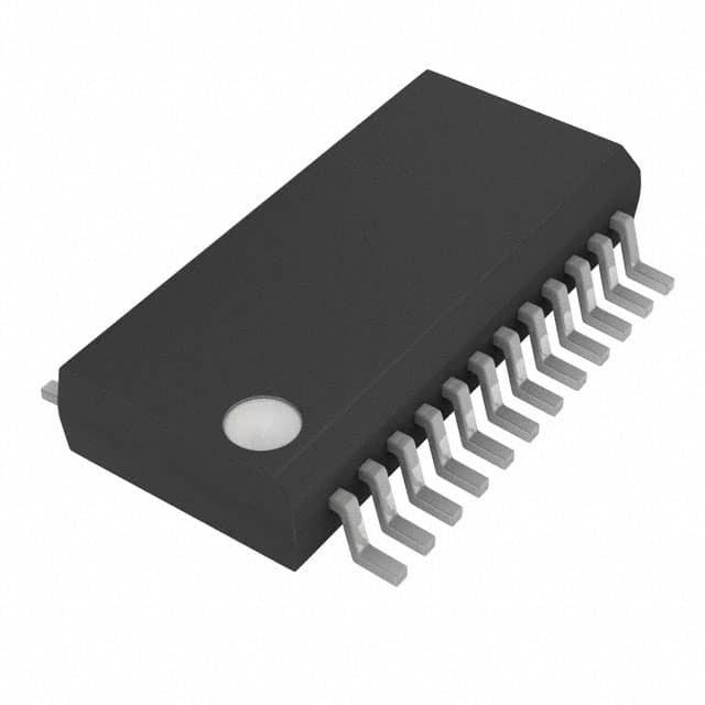
- Part No.:
- TLC5949DBQR
- Manufacturer:
- Texas Instruments
- Category:
- LED Drivers
- Package:
- 24-SSOP (0.154", 3.90mm Width)
- Datasheet:
-
 TLC5949DBQR.pdf
- Description:
- IC LED DRVR LIN PWM 45MA 24SSOP
- Quantity:
- Payment:

- Shipping:

Inventory:2,681
Please send an inquiry. Send us your inquiry, and we will respond immediately.
Product details
Overview
TLC5949DBQR from Texas Instruments is a 16-channel, 12-bit enhanced-spectrum PWM LED driver with integrated pre-thermal warning, LED open/short detection, and 7-bit global brightness control. It delivers ±0.6% (typ) channel-to-channel current accuracy, supports up to 45 mA per output, and operates from 3.0 V to 3.6 V supply voltage. It is used in high-reliability LED video displays requiring invisible fault detection and daisy-chainable grayscale control.
For engineers reviewing the TLC5949DBQR datasheet, TLC5949DBQR pinout, TLC5949DBQR application, or TLC5949DBQR equivalent, key selection criteria include its 12-bit ES-PWM architecture, 33 MHz data transfer rate, four-channel grouped delay switching for inrush mitigation, LOD/LSD/PTW/TEF error flag reporting via serial interface, and compatibility with 1.1 kΩ–25.4 kΩ IREF resistors for 2–45 mA sink current tuning.
Technical Context
The TLC5949DBQR implements dual-stage grayscale control: a 12-bit per-channel PWM counter driven by GSCLK (up to 33 MHz), and a 7-bit global brightness register scaling all outputs from 25% to 100% of IOLCMax. Its ES-PWM mode spreads spectral energy to reduce visible flicker and EMI versus conventional PWM.
Error detection is fully integrated and non-intrusive: LED open detection (LOD) thresholds are programmable across four levels (0.25–1.25 V), short detection (LSD) scales with VCC, and thermal flags (PTW at 138°C typ, TEF at 150°C) trigger status readback via SOUT without display interruption. All diagnostics operate during active GS data latching.
Key Specifications
| Parameter | Value and Actual Design Meaning |
|---|---|
| Output channels | 16 constant-current sink outputs, each individually controllable with 12-bit grayscale resolution (4096 steps) |
| Sink current range | 2 mA to 45 mA per channel, set externally via IREF resistor (1.13 kΩ–25.4 kΩ) |
| Global BC resolution | 7-bit (128 steps), adjusts all outputs simultaneously from 25% to 100% of max current |
| Data clock rate | 33 MHz SCLK and GSCLK - enables full 193-bit frame write in ≤5.8 µs |
| Current accuracy | ±0.6% (typ) channel-to-channel, ±1% (typ) device-to-device at +25°C |
| Operating temperature | –40°C to +85°C ambient; junction limit +125°C continuous, +150°C shutdown |
| Supply voltage | 3.0 V to 3.6 V VCC - optimized for low-noise 3.3 V systems |
Pinout & Package
Package: 24-pin SSOP (DBQ), 0.15 mm pitch, exposed PowerPAD not present (DBQ variant). Thermal resistance θJA = 80.4°C/W.
| Pin/Terminal | Circuit Role | Design Meaning |
|---|---|---|
| GND (Pin 1) | Power ground reference | Primary return path for all output sink currents and internal logic; must be low-impedance connection to minimize voltage offset errors |
| SIN (Pin 2) | Serial data input | LSB-first 193-bit shift register input; accepts GS, BC, and control data; compatible with 3.3 V CMOS logic |
| SCLK (Pin 3) | Data shift clock | Rising-edge triggered; clocks SIN data into shift register and shifts SOUT data out; max 33 MHz |
| LAT (Pin 4) | Data latch control | Rising edge latches shift register contents into first GS or control data latch; initiates display timing reset when TMGRST = 1 |
| OUT0–OUT15 (Pins 5–20) | Constant-current sink outputs | 16 independent N-channel sinks; each drives LED cathode; supports parallel connection for higher current |
| GSCLK (Pin 21) | Grayscale clock input | Drives 12-bit PWM counter; rising edge increments GS counter; disabled during BLANK = 1 |
| SOUT (Pin 22) | Status data output | Serial readback of LOD, LSD, OLD, ISF, PTW, TEF flags after LAT pulse; MSB of shift register |
| IREF (Pin 23) | Reference current terminal | Connects external resistor to GND; sets IOLCMax; shorting to GND forces all outputs off and asserts ISF flag |
| VCC (Pin 24) | Positive supply | 3.0–3.6 V power input; powers logic, drivers, and internal reference; decoupling capacitor required |
Key Features
| Feature | Design Value |
|---|---|
| Invisible LED fault detection | LOD and LSD operate during active display without blanking or visual artifacts; four programmable LOD thresholds enable robust margining |
| Pre-thermal warning (PTW) | Asserts flag at 138°C (typ) - provides 12°C headroom before thermal shutdown (150°C), enabling proactive thermal management |
| Four-channel grouped delay switching | Staggers turn-on of OUT0–OUT3, OUT4–OUT7, OUT8–OUT11, OUT12–OUT15 to limit inrush current and reduce peak VCC demand |
| Enhanced Spectrum (ES) PWM | Spreads PWM energy across frequency domain vs conventional PWM, reducing EMI and visible flicker in high-refresh-rate displays |
| Auto display repeat & refresh | Eliminates need for continuous host data streaming; internal timing controller maintains stable output once loaded |
Applications
| LED Video Displays | LED Signboards |
|---|---|
Use Scenario: Indoor full-color video wall with 1920×1080 resolution using RGB SMD2835 LEDs at 3000 nits brightness. IC Role / Device Role / Timing Role: Primary grayscale driver per 16-LED segment; receives serialized GS/BC data over daisy-chained SCLK/SIN/LAT; generates precise 12-bit PWM per channel synchronized to GSCLK. Use Value: ±0.6% channel-to-channel current matching ensures uniform color field across panels; ES-PWM minimizes visible scanning lines at 120 Hz refresh. | Use Scenario: Outdoor highway variable-message sign with 128×32 pixel matrix and wide operating temperature range (–40°C to +85°C). IC Role / Device Role / Timing Role: Constant-current sink driver for high-brightness red/green/yellow LEDs; uses PTW and TEF flags for predictive thermal derating and automatic brightness adjustment. Use Value: Pre-thermal warning enables dynamic brightness reduction before thermal shutdown; LOD/LSD detection prevents false pixel failure alarms during voltage transients. |
| Architectural Lighting Systems | Industrial HMI Panels |
Use Scenario: Tunable-white linear lighting fixture with 48 individually dimmed zones, controlled via DALI-2 gateway. IC Role / Device Role / Timing Role: Local LED driver node receiving GS/BC commands via isolated UART-to-SPI bridge; leverages auto-display-repeat to maintain smooth fade transitions without host intervention. Use Value: Power-save mode reduces VCC current to <40 µA when outputs idle - extends standby battery life in wireless-controlled fixtures. | Use Scenario: Factory-floor operator panel with 16 status indicators (RUN/ALARM/FAULT/READY), exposed to ESD and vibration. IC Role / Device Role / Timing Role: Fault-tolerant LED driver with built-in diagnostics; reads LOD/LSD/ISF flags via SOUT after each LAT pulse to confirm LED integrity before display update. Use Value: Invisible detection mode (IDM) reports faults without disrupting indicator state; charged-device-model ESD rating (2000 V) withstands industrial handling. |
Equivalent & Alternatives
The following parts are listed as comparable options for similar LED driver applications.
| Alternative Part | Technical Difference | Application Difference | Selection Advice |
|---|---|---|---|
| TLC5947DBQR | 16-channel, 12-bit, but lacks PTW, TEF, LOD/LSD diagnostics; no ES-PWM; lower max sink current (30 mA) | No thermal or LED fault reporting; unsuitable for safety-critical or predictive maintenance use cases | Select when cost sensitivity outweighs diagnostic requirements and thermal margins are well-controlled |
| MAX7219CWG+ | 8-channel, 8-bit, SPI interface only; includes scan-limiting and BCD decode; no current accuracy spec or thermal flags | Designed for 7-segment/matrix displays, not high-fidelity grayscale LED video; no per-channel current tuning | Choose for simple numeric/character displays where grayscale depth and current precision are secondary |
Compared with TLC5947DBQR and MAX7219CWG+, the TLC5949DBQR uniquely combines 12-bit ES-PWM, full diagnostic flag set (LOD/LSD/PTW/TEF), and 45 mA sink capability - making it the only option among the three qualified for high-reliability, high-fidelity LED video applications demanding invisible fault detection and thermal predictability.
Availability
TLC5949DBQR is available at Aetrix Electronics and suitable for LED video displays, outdoor signboards, architectural lighting systems, and industrial HMI panels requiring stable component supply, long-term lifecycle support, and guaranteed traceable sourcing.
Supply support for TLC5949DBQR includes scheduled delivery planning, volume procurement assistance, BOM continuity management, traceable sourcing, and lifecycle availability coordination for OEM customers, industrial embedded developers, connected-device designers, and electronics production programs.
Manufacturer
Texas Instruments is a global semiconductor leader specializing in analog, embedded processing, and high-reliability ICs for industrial, automotive, and communications markets.
The TLC5949 belongs to TI's high-precision LED driver product line, engineered specifically for applications demanding invisible fault detection, thermal predictability, and 12-bit grayscale fidelity in mission-critical visual systems.
FAQ
What is the maximum sink current per channel for the TLC5949DBQR?
The TLC5949DBQR supports a maximum sink current of 45 mA per channel (OUT0–OUT15) when configured with RIREF = 1.13 kΩ and global brightness control (BC) set to 7Fh (127). Current is programmable from 2 mA to 45 mA using an external resistor between IREF and GND, with typical accuracy of ±0.6% channel-to-channel at +25°C. The TLC5949DBQR maintains this specification across its full operating temperature range of –40°C to +85°C.
How does the TLC5949DBQR implement invisible LED open and short detection?
The TLC5949DBQR performs invisible LED open detection (LOD) and LED short detection (LSD) during normal grayscale operation without interrupting display output. LOD thresholds are configurable across four levels (0.25 V to 1.25 V), while LSD thresholds scale with VCC (0.35×VCC to 0.65×VCC). Detection results are reported via the SOUT pin after each LAT pulse as part of the status information data (SID) register. This allows real-time fault monitoring in the TLC5949DBQR without visible flicker or blanking.
What is the function of the GSCLK and SCLK pins on the TLC5949DBQR?
On the TLC5949DBQR, GSCLK (Pin 21) is the grayscale clock input that drives the 12-bit PWM counter - each rising edge increments the counter for per-channel duty-cycle generation. SCLK (Pin 3) is the serial data shift clock - its rising edge shifts data into the 193-bit common shift register from SIN and shifts status bits out via SOUT. Both clocks support up to 33 MHz operation, but serve entirely separate functions: GSCLK controls PWM timing, while SCLK controls data loading and status readback in the TLC5949DBQR.
Does the TLC5949DBQR support daisy-chaining, and how is it implemented?
Yes, the TLC5949DBQR supports seamless daisy-chaining for multi-device systems. SOUT of one device connects directly to SIN of the next, while shared SCLK, LAT, GSCLK, and VCC/GND lines drive the chain. Each TLC5949DBQR consumes 193 bits per frame (128 bits GS + 7 bits BC + 58 bits control), and the LAT pulse latches data into the first device's registers before propagating remaining bits downstream. This architecture enables scalable LED matrix control without additional address decoding logic in the TLC5949DBQR system.
What thermal protection features does the TLC5949DBQR provide?
The TLC5949DBQR integrates two thermal protection mechanisms: pre-thermal warning (PTW) and thermal error flag (TEF). PTW asserts at 138°C (typical junction temperature), providing 12°C margin before TEF triggers at 150°C, initiating thermal shutdown. Both flags are readable via SOUT after LAT, enabling host firmware to initiate derating (e.g., reduce BC or disable segments) before shutdown. The TLC5949DBQR also specifies TJ(max) = +125°C for continuous operation and includes thermal metrics (θJA = 80.4°C/W for DBQ package) for board-level thermal design.
TLC5949DBQR Specifications
- Product attributes
- Attribute value
- Manufacturer:
- Texas Instruments
- Series:
- -
- Package/Case:
- 24-SSOP (0.154", 3.90mm Width)
- Packaging:
- Tape & Reel (TR)
- Product Status:
- Active
- Type:
- Linear
- Topology:
- Shift Register
- Internal Switch(s):
- Yes
- Number of Outputs:
- 16
- Voltage - Supply (Min):
- 3V
- Voltage - Supply (Max):
- 3.6V
- Voltage - Output:
- 10V
- Current - Output / Channel:
- 45mA
- Frequency:
- 33MHz
- Dimming:
- PWM
- Applications:
- Signage
- Operating Temperature:
- -40°C ~ 85°C (TA)
- Grade:
- -
- Qualification:
- -
- Mounting Type:
- Surface Mount
- Supplier Device Package:
- 24-SSOP
TLC5949DBQR FAQ
1.How can I place an order for TLC5949DBQR through Aetrix?
Please submit a Request for Quotation (RFQ) for TLC5949DBQR on Aetrix. Our sales agent will provide a competitive quotation and guide you through the order confirmation once you accept the terms.
2.Are the price and stock information for TLC5949DBQR reliable?
The price and inventory of TLC5949DBQR are updated periodically and may fluctuate due to market conditions. Stock and pricing data are typically refreshed every 24 hours. Quotation validity for TLC5949DBQR is usually 5 days.
3.What payment methods are accepted for TLC5949DBQR?
We accept Wire Transfer, PayPal, Credit Card, Western Union, MoneyGram, and Escrow for TLC5949DBQR transactions.
Note: Certain payment methods may incur a processing fee.
4.How is shipping managed for TLC5949DBQR?
TLC5949DBQR orders can be shipped via leading logistics carriers, including DHL, UPS, FedEx, TNT, or Registered Mail.
Once your TLC5949DBQR order is processed, you will receive an email with the shipment details and tracking number.
Note: Tracking information may take up to 24 hours to appear. Express delivery typically takes 3–5 business days.
5.How can I obtain technical support or documentation for TLC5949DBQR?
For technical support, including TLC5949DBQR datasheets, pinout diagrams, or application guidance, please contact our engineering support team. They can provide detailed documentation and assistance for your TLC5949DBQR requirements.
6.How does Aetrix verify that TLC5949DBQR is sourced from the original manufacturer or authorized distributors?
All TLC5949DBQR products on Aetrix are procured from qualified distributors and authorized channels. Our dedicated quality assurance team conducts strict verification, including traceability checks and, if necessary, third-party testing. This ensures that TLC5949DBQR meets industry standards.
7.What is the process for return or replacement of TLC5949DBQR?
All TLC5949DBQR units undergo pre-shipment inspection (PSI). If there is an issue with TLC5949DBQR, returns or replacements are accepted under the following conditions:
1.Quantity discrepancies, incorrect items, or visible external defects (such as breakage or corrosion), acknowledged by Aetrix.
2.The issue is reported within 90 days of delivery.
3.The TLC5949DBQR part is unused and in its original packaging.
Return procedure for TLC5949DBQR:
1.Submit a request within 90 days.
2.Obtain a Return Material Authorization (RMA) from Aetrix.
TLC5949DBQR Tags

-
BCR402RE6327HTSA1
Infineon Technologies

-
BCR430UXTSA2
Infineon Technologies

-
BCR420UE6433HTMA1
Infineon Technologies
-
BCR420UE6327HTSA1
Infineon Technologies
-
BCR421UE6327HTSA1
Infineon Technologies

-
LYT1604D-TL
Power Integrations

-
HV9910CLG-G
Microchip Technology

-
CL2N8-G
Microchip Technology

-
BCR420UW6-7
Diodes Incorporated
-
BCR421UW6-7
Diodes Incorporated

-
BCR420UFD-7
Diodes Incorporated
-
BCR421UFD-7
Diodes Incorporated
Tech Hub

A practical engineering guide to 3.3V and 5V logic compatibility, input thresholds, resistor dividers, translator ICs, MOSFET level shifting, I2C pull-ups, timing limits and power-sequencing risks.

The 74HC595 uses push-pull logic outputs, while the TPIC6B595 uses 50 V open-drain DMOS sinks for higher-power loads. This guide compares timing, current limits, 3.3 V interfacing, load wiring, thermal…

The 74HC595 converts serial data into eight stable parallel outputs. This guide covers pin functions, shift and storage timing, OE and MR behavior, drive-current limits, cascading, voltage compatibilit…

A technical comparison of level-sensitive latches and edge-triggered flip-flops, covering timing windows, setup and hold limits, master–slave operation, time borrowing, race-through, HDL inference and…

A D latch stores one bit while Enable controls when data can pass. This reference covers gate-level operation, truth tables, transparency, setup and hold timing, LE versus OE, common ICs and practical …

An SR latch stores one bit through cross-coupled feedback. This engineering reference covers NOR and NAND implementations, truth tables, forbidden-state recovery, gated operation, switch debouncing, fa…

Latch circuits retain one bit through feedback. This technical reference covers SR and D latches, truth tables, transparency, timing limits, latch-versus-flip-flop behavior, applications and common log…

An engineering guide to LED driver operation, constant-current and constant-voltage outputs, linear and switching topologies, dimming, IC selection, calculations, replacement compatibility, and fault c…

Operational amplifier guide covering op amp basics, feedback, ideal vs real op amps, common configurations, buffer circuits, offset, bias current, gain-bandwidth, slew rate, rail-to-rail limits and sel…

Jumper cables guide covering safe connection order, red and black clamp placement, final ground connection, cable gauge, length, clamp quality, copper vs CCA cables, jump starter comparison and battery…


