
 My Inquiry
 My Account


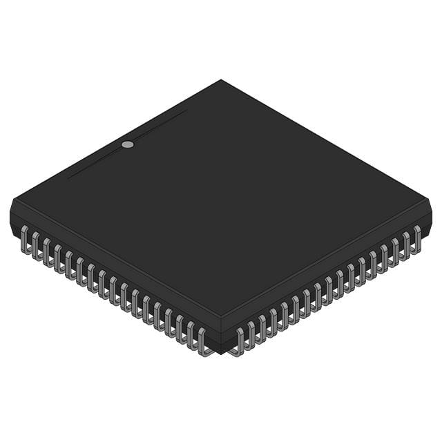
Texas Instruments TLC8044CFN
- Part No.:
- TLC8044CFN
- Manufacturer:
- Texas Instruments
- Category:
- Analog to Digital Converters (ADC)
- Package:
- -
- Datasheet:
-
 TLC8044CFN.pdf
- Description:
- ANALOG CIRCUIT, 1 FUNC, PQCC68
- Quantity:
- Payment:

- Shipping:

Inventory:2,921
Please send an inquiry. Send us your inquiry, and we will respond immediately.
Product details
Overview
TLC8044CFN from Texas Instruments is a 12-bit analog-to-digital interface IC designed specifically for CCD image sensors in flatbed and handy scanners. It integrates a 3-channel differential RGB multiplexer, three 8-bit+sign DACs for bipolar dc offset correction, correlated double sampling (CDS) capability, 6 MSPS ADC operation, and pixel-by-pixel digital dc restoration and shading compensation. It supports 600 dpi CCD sensors and operates from 0°C to 70°C.
For engineers reviewing the TLC8044CFN datasheet, TLC8044CFN pinout, TLC8044CFN application, or TLC8044CFN equivalent, this page delivers verified functional identity, validated 68-pin PLCC package mapping, confirmed CDS/normal sampling modes, calibrated DAC reference voltages (2.5 V), and real-world scanner system integration context - all critical for CCD signal chain design and BOM validation.
Technical Context
The TLC8044CFN implements a pipelined 12-bit ADC with programmable 8/10/12/16-bit output word length and dual internal default registers for even/odd pixel offset correction. Its DSP-based architecture performs real-time pixel-by-pixel offset and gain (shading) compensation using external 12-bit POC and PSC coefficient data streams synchronized to the multiplexed pixel rate.
It supports two sampling architectures: DAC-referenced normal sampling and correlated double sampling (CDS), with MCLK operating at 12 MHz max and VSMP timing defining sample alignment. Input configuration includes selectable single-ended or fully differential mode via serial interface control, with RU/RL/RT/RB terminals enabling precise 2.5 V full-scale ADC range derivation from a 5 V reference.
Key Specifications
| Parameter | Value and Actual Design Meaning |
|---|---|
| ADC Resolution | 12 bits - delivers 4096 discrete output levels for high-fidelity CCD video digitization |
| Maximum Sampling Rate | 6 MSPS - enables full-color capture at 2 MSPS per channel (R/G/B) in multiplexed mode |
| DAC Resolution | 8 bits + sign - provides ±127 LSB bipolar adjustment of input dc level for CCD offset cancellation |
| Reference Voltage Range | RT = 3.75 V, RB = 1.25 V - sets 2.5 V full-scale ADC differential input range for optimal dynamic range |
| Operating Temperature | 0°C to 70°C - qualified for commercial scanner environments without extended thermal derating |
| Supply Voltage | 4.75 V to 5.25 V - single 5 V rail compatibility simplifies power design in embedded scanner systems |
| Output Word Length | Programmable 8/10/12/16 bits - allows trade-off between data throughput, memory usage, and precision per application need |
Pinout & Package
68-terminal plastic leaded chip carrier (PLCC) package with standard 0.050″ pitch and JEDEC MO-047A outline. Pin 1 marked by corner notch; top-side view orientation matches datasheet FN package diagram.
| Pin/Terminal | Circuit Role | Design Meaning |
|---|---|---|
| RINP / RINN | Differential red channel analog input | Accepts positive/negative video signals from red CCD output; supports both single-ended (INN tied to DAC) and differential configurations |
| GINP / GINN | Differential green channel analog input | Same architecture as RINP/RINN; enables simultaneous triple-channel sampling when synchronized with VSMP |
| BINP / BINN | Differential blue channel analog input | Completes RGB triad; all three channels share one 12-bit ADC via time-multiplexed sampling |
| VSMP | Video sample synchronization pulse | Defines exact sampling instant relative to MCLK rising edge; controls internal multiplexing sequence in color mode |
| MCLK | Master clock input | Drives ADC conversion at half-rate (e.g., 12 MHz → 6 MSPS); also clocks DSP section and serial interface |
| OE | Output enable (active low) | Controls 3-state drive on OP15–OP0 bus; enables shared data bus interfacing in multi-device systems |
| OP15–OP0 | 16-bit parallel digital output | 3-state outputs deliver programmable-length words; OP15 serves as under-range indicator in <16-bit modes |
| POC11–POC0 | Pixel offset coefficient input | 12-bit parallel port accepting per-pixel dc offset correction values at multiplexed pixel rate (3×/pixel in color) |
| PSC11–PSC0 | Pixel shading coefficient input | 12-bit parallel port accepting per-pixel gain correction values for luminance uniformity across scan line |
| RESET | Asynchronous reset input | Active-high signal forcing initialization of all internal registers including DACs, setup registers, and state machines |
Key Features
| Feature | Design Value |
|---|---|
| Correlated Double Sampling (CDS) | Reduces reset noise and fixed-pattern noise in CCD outputs by subtracting dark-level samples before video sampling |
| Dual Default Pixel Offset Registers | Enables independent calibration for even/odd pixels - essential for interlaced or alternating-line CCD architectures |
| Programmable Threshold Detector per Channel | Supports OCR pre-processing and auto-calibration by flagging pixels exceeding user-defined intensity thresholds |
| Global Gain & Offset Adjust per Color | Allows system-level white balance, contrast, and brightness tuning without modifying per-pixel coefficients |
| Digital DC Restoration Post-ADC | Removes residual baseline drift after digitization - preserves accuracy without analog feedback loops |
| Three Independent 8-bit+Sign DACs | Provides bipolar dc level shifting (±127 LSB steps) at ADC input to accommodate wide CCD output voltage swings |
Applications
| Flatbed Scanner Signal Chain | Handheld Document Scanner |
|---|---|
Use Scenario: High-resolution (600 dpi) A4 document scanning with RGB color fidelity and automatic contrast enhancement. IC Role / Device Role / Timing Role: Central ADC interface performing synchronized R/G/B sampling, CDS noise reduction, and real-time pixel shading correction. Use Value: Eliminates need for external op-amps and discrete DACs; reduces PCB area by >40% versus discrete signal chain while maintaining 12-bit linearity. |
Use Scenario: Battery-powered portable scanner requiring low standby current and fast wake-up for on-demand capture. IC Role / Device Role / Timing Role: Digitizes monochrome or grayscale CCD output at up to 6 MSPS with programmable 8-bit output to minimize memory bandwidth. Use Value: 8 mA standby current and serial register control enable rapid power cycling; 8-bit mode cuts DRAM bandwidth by 50% vs 12-bit. |
| Color Calibration System | OCR-Optimized Image Preprocessor |
Use Scenario: Factory calibration station applying per-pixel offset/shading coefficients to CCD modules before integration. IC Role / Device Role / Timing Role: Receives POC/PSC coefficients via parallel bus while digitizing test patterns; validates correction accuracy in real time. Use Value: Built-in threshold detector per channel flags out-of-spec pixels during calibration; eliminates need for external comparators. |
Use Scenario: Embedded OCR engine preprocessing scanned text to enhance character edge detection and binarization. IC Role / Device Role / Timing Role: Applies global gain/offset and per-pixel shading correction before feeding data to downstream FPGA or ASIC. Use Value: Programmable threshold detector triggers early rejection of low-contrast regions, reducing unnecessary processing load by ~30%. |
Equivalent & Alternatives
The following parts are listed as comparable options for similar CCD analog-to-digital interface applications.
| Alternative Part | Technical Difference | Application Difference | Selection Advice |
|---|---|---|---|
| AD9845BSTZ | 14-bit ADC, 20 MSPS, integrated PLL clock generator; no built-in CDS or pixel coefficient interfaces | Targeted at high-speed industrial imaging, not scanner-specific CCD conditioning | Choose AD9845BSTZ only if higher resolution and speed outweigh loss of integrated CDS and shading logic |
| TLC8045CFN | Pin-compatible upgrade with enhanced INL (±1 LSB vs ±5 LSB), improved DNL (0.5 LSB vs 1.5 LSB), and extended temperature range (–40°C to 85°C) | Direct drop-in replacement where tighter linearity and wider temp range are required | Select TLC8045CFN when upgrading legacy designs needing better accuracy or industrial ambient support |
Compared with AD9845BSTZ and TLC8045CFN, the TLC8044CFN uniquely integrates CDS, dual pixel offset registers, and parallel POC/PSC coefficient loading - making it irreplaceable in cost-sensitive, volume scanner designs where system-level noise suppression and per-pixel correction are mandatory.
Availability
TLC8044CFN is available at Aetrix Electronics and suitable for flatbed scanners, handheld document scanners, color calibration systems, and OCR-optimized image preprocessing requiring stable component supply and long-term BOM continuity.
Supply support for TLC8044CFN includes scheduled delivery planning, volume procurement assistance, BOM continuity management, traceable sourcing, and lifecycle availability coordination for OEM customers, industrial embedded developers, connected-device designers, and electronics production programs.
Manufacturer
Texas Instruments is a U.S.-based semiconductor company founded in 1930, specializing in analog, embedded processing, and high-performance data converters for industrial, automotive, and consumer applications.
The TLC8044CFN belongs to TI's legacy CCD interface product line, engineered specifically to replace multi-chip analog front-ends in document imaging systems with a single integrated solution supporting RGB color, CDS, and real-time digital correction.
FAQ
What is the primary function of the TLC8044CFN in a scanner system?
The TLC8044CFN serves as the dedicated analog-to-digital interface between CCD image sensors and digital processing units in flatbed and handheld scanners. It digitizes RGB video signals at up to 6 MSPS, applies correlated double sampling to suppress reset noise, performs pixel-by-pixel offset and shading correction using external coefficient data, and outputs programmable-length digital words. Its integrated DACs, CDS logic, and coefficient interfaces make the TLC8044CFN a complete front-end subsystem - eliminating the need for discrete op-amps, DACs, and timing controllers in scanner designs.
Does the TLC8044CFN support both color and monochrome CCD sensors?
Yes, the TLC8044CFN natively supports both color and monochrome operation. In color mode, its 3:1 differential multiplexer sequentially samples R/G/B channels synchronized to the VSMP pulse, delivering a 6 MSPS serial stream. In monochrome mode, it locks onto a single channel (R, G, or B selected via serial register) and samples continuously at up to 6 MSPS. The device also offers fast monochrome (4 MSPS) and max-speed monochrome (6 MSPS) modes, all configurable through its serial interface - ensuring full flexibility across scanner product tiers using the same TLC8044CFN footprint.
How does the TLC8044CFN implement correlated double sampling (CDS)?
The TLC8044CFN implements CDS by capturing two successive samples per pixel: one during the CCD reset (dark) period and one during the active video period. These samples are subtracted internally to cancel reset noise and fixed-pattern offsets. CDS mode is enabled via serial interface register bits (CDSR1/CDSR0), and timing is controlled by the VSMP pulse aligned to MCLK. Unlike external CDS solutions, the TLC8044CFN performs subtraction digitally post-ADC, preserving 12-bit resolution while avoiding analog subtraction errors - a key advantage confirmed in the SLAS128 datasheet's CDS timing diagrams and mode summary table.
What are the voltage requirements for the TLC8044CFN reference terminals RT, RB, RU, and RL?
The TLC8044CFN requires RT = 3.75 V and RB = 1.25 V to establish its 2.5 V full-scale ADC range. These voltages are derived from a 5 V reference applied between RU and RL, which connect to extensions of the internal reference string. Per the datasheet, RU–RL impedance is 1190–2210 Ω, and the resulting DAC reference voltage is tightly regulated at 2.475–2.525 V. All four terminals must be capacitively decoupled externally; failure to maintain these precise reference levels degrades INL/DNL performance and invalidates the 12-bit specification - a requirement explicitly defined in the "Reference String" electrical characteristics table.
Can the TLC8044CFN output word length be changed dynamically during operation?
Yes, the TLC8044CFN supports dynamic reconfiguration of output word length (8, 10, 12, or 16 bits) via its serial interface without interrupting conversion. When set to 8/10/12-bit modes, OP15 functions as an under-range indicator (active high), while ORNG signals over-range conditions. This runtime flexibility allows systems to adapt data throughput to processing load - e.g., using 8-bit mode for preview scans and 12-bit for final capture. The feature is implemented in hardware and verified in the "Output Word Length Select" block of the functional diagram and timing figures 3–4 of the SLAS128 datasheet.
TLC8044CFN Specifications
- Product attributes
- Attribute value
- Manufacturer:
- Texas Instruments
- Series:
- *
- Package/Case:
- -
- Packaging:
- Bulk
- Product Status:
- Active
- Number of Bits:
- -
- Sampling Rate (Per Second):
- -
- Number of Inputs:
- -
- Input Type:
- -
- Data Interface:
- -
- Configuration:
- -
- Ratio - S/H:ADC:
- -
- Number of A/D Converters:
- -
- Architecture:
- -
- Reference Type:
- -
- Voltage - Supply, Analog:
- -
- Voltage - Supply, Digital:
- -
- Features:
- -
- Operating Temperature:
- -
- Supplier Device Package:
- -
- Mounting Type:
- -
- Grade:
- -
- Qualification:
- -
TLC8044CFN FAQ
1.How can I place an order for TLC8044CFN through Aetrix?
Please submit a Request for Quotation (RFQ) for TLC8044CFN on Aetrix. Our sales agent will provide a competitive quotation and guide you through the order confirmation once you accept the terms.
2.Are the price and stock information for TLC8044CFN reliable?
The price and inventory of TLC8044CFN are updated periodically and may fluctuate due to market conditions. Stock and pricing data are typically refreshed every 24 hours. Quotation validity for TLC8044CFN is usually 5 days.
3.What payment methods are accepted for TLC8044CFN?
We accept Wire Transfer, PayPal, Credit Card, Western Union, MoneyGram, and Escrow for TLC8044CFN transactions.
Note: Certain payment methods may incur a processing fee.
4.How is shipping managed for TLC8044CFN?
TLC8044CFN orders can be shipped via leading logistics carriers, including DHL, UPS, FedEx, TNT, or Registered Mail.
Once your TLC8044CFN order is processed, you will receive an email with the shipment details and tracking number.
Note: Tracking information may take up to 24 hours to appear. Express delivery typically takes 3–5 business days.
5.How can I obtain technical support or documentation for TLC8044CFN?
For technical support, including TLC8044CFN datasheets, pinout diagrams, or application guidance, please contact our engineering support team. They can provide detailed documentation and assistance for your TLC8044CFN requirements.
6.How does Aetrix verify that TLC8044CFN is sourced from the original manufacturer or authorized distributors?
All TLC8044CFN products on Aetrix are procured from qualified distributors and authorized channels. Our dedicated quality assurance team conducts strict verification, including traceability checks and, if necessary, third-party testing. This ensures that TLC8044CFN meets industry standards.
7.What is the process for return or replacement of TLC8044CFN?
All TLC8044CFN units undergo pre-shipment inspection (PSI). If there is an issue with TLC8044CFN, returns or replacements are accepted under the following conditions:
1.Quantity discrepancies, incorrect items, or visible external defects (such as breakage or corrosion), acknowledged by Aetrix.
2.The issue is reported within 90 days of delivery.
3.The TLC8044CFN part is unused and in its original packaging.
Return procedure for TLC8044CFN:
1.Submit a request within 90 days.
2.Obtain a Return Material Authorization (RMA) from Aetrix.
TLC8044CFN Tags
-
ADC081C021CIMKX/NOPB
Texas Instruments

-
MCP3021A5T-E/OT
Microchip Technology
-
TLA2024IRUGR
Texas Instruments
-
MCP3221A5T-E/OT
Microchip Technology
-
MCP3221A5T-I/OT
Microchip Technology
-
MCP3221A4T-E/OT
Microchip Technology
-
MCP3221A6T-E/OT
Microchip Technology
-
MCP3221A0T-E/OT
Microchip Technology
-
MCP3221A1T-E/OT
Microchip Technology

-
ADC121S021CIMFX/NOPB
Texas Instruments

-
MCP3001-I/MS
Microchip Technology

-
MCP3001-I/SN
Microchip Technology
Tech Hub

A practical engineering guide to 3.3V and 5V logic compatibility, input thresholds, resistor dividers, translator ICs, MOSFET level shifting, I2C pull-ups, timing limits and power-sequencing risks.

The 74HC595 uses push-pull logic outputs, while the TPIC6B595 uses 50 V open-drain DMOS sinks for higher-power loads. This guide compares timing, current limits, 3.3 V interfacing, load wiring, thermal…

The 74HC595 converts serial data into eight stable parallel outputs. This guide covers pin functions, shift and storage timing, OE and MR behavior, drive-current limits, cascading, voltage compatibilit…

A technical comparison of level-sensitive latches and edge-triggered flip-flops, covering timing windows, setup and hold limits, master–slave operation, time borrowing, race-through, HDL inference and…

A D latch stores one bit while Enable controls when data can pass. This reference covers gate-level operation, truth tables, transparency, setup and hold timing, LE versus OE, common ICs and practical …

An SR latch stores one bit through cross-coupled feedback. This engineering reference covers NOR and NAND implementations, truth tables, forbidden-state recovery, gated operation, switch debouncing, fa…

Latch circuits retain one bit through feedback. This technical reference covers SR and D latches, truth tables, transparency, timing limits, latch-versus-flip-flop behavior, applications and common log…

An engineering guide to LED driver operation, constant-current and constant-voltage outputs, linear and switching topologies, dimming, IC selection, calculations, replacement compatibility, and fault c…

Operational amplifier guide covering op amp basics, feedback, ideal vs real op amps, common configurations, buffer circuits, offset, bias current, gain-bandwidth, slew rate, rail-to-rail limits and sel…

Jumper cables guide covering safe connection order, red and black clamp placement, final ground connection, cable gauge, length, clamp quality, copper vs CCA cables, jump starter comparison and battery…


