
 My Inquiry
 My Account


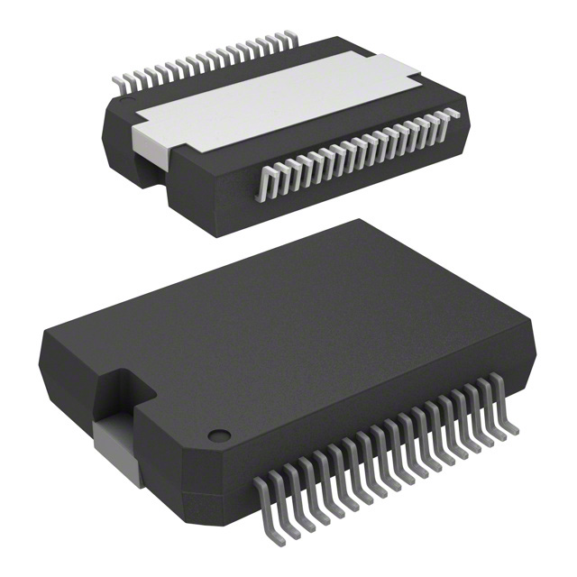
Infineon Technologies TLE8261-2E
- Part No.:
- TLE8261-2E
- Manufacturer:
- Infineon Technologies
- Category:
- Specialized ICs
- Package:
- 36-BSSOP (0.295", 7.50mm Width) Exposed Pad
- Datasheet:
-
 TLE8261-2E.pdf
- Description:
- IC TRANSCEIVER DSO36-38
- Quantity:
- Payment:

- Shipping:

Inventory:4,609
Please send an inquiry. Send us your inquiry, and we will respond immediately.
Product details
Overview
TLE8261-2E from Infineon Technologies is a universal System Basis Chip (SBC) for automotive CAN networks, integrating a high-speed CAN transceiver (ISO 11898-2/5 compliant), three independent 5 V LDO regulators (Vcc1µC/Vcc2/Vcc3), SPI-configurable watchdog/reset supervision, wake-up input, and three open-drain Limp Home outputs. It operates from 5.5 V to 27 V supply, supports -40 °C to +150 °C ambient, and delivers 200 mA per main regulator with ±2% output accuracy.
For engineers reviewing the TLE8261-2E datasheet, TLE8261-2E pinout, TLE8261-2E application, or TLE8261-2E equivalent, this device serves as a complete power management and communication interface solution for body control modules, gateway ECUs, and battery-connected automotive subsystems requiring fail-safe operation, low quiescent current in Stop/Sleep modes (<30 µA), and bus-initiated wake-up capability.
Technical Context
The TLE8261-2E implements a state-machine-driven SBC architecture with dedicated hardware blocks: a HS-CAN transceiver supplied by VccHSCAN, three regulated outputs (Vcc1µC for MCU, Vcc2 for internal CAN cell, Vcc3 configurable up to 400 mA via external PNP), and SPI-controlled supervision logic including window watchdog (16–1024 ms timeout), reset generation, and interrupt management with timing filters.
Its wake-up system supports bi-level-sensitive WK input, cyclic wake in Stop Mode, and bus wake via CAN message detection; all wake sources are individually inhibitable. The Limp Home circuitry provides three independent open-drain outputs with dedicated safety logic, including 1.25 Hz side-indicator and 100 Hz PWM signals, and failsafe activation on undervoltage or thermal fault.
Key Specifications
| Parameter | Value and Actual Design Meaning |
|---|---|
| Supply Voltage Range | 5.5 V to 27 V - Enables direct connection to automotive battery with load-dump tolerance. |
| Vcc1µC Output | 5 V ±2%, 200 mA - Powers microcontroller and RF receiver with tight regulation for stable digital operation. |
| CAN Data Rate | Up to 1 MBaud - Supports high-speed CAN FD-ready physical layer in legacy CAN networks. |
| Quiescent Current (Sleep) | <30 µA - Enables always-on battery-connected applications without excessive drain. |
| Watchdog Timeout Range | 16 ms to 1024 ms, SPI-configurable - Allows precise system-level timing control for MCU health monitoring. |
| Limp Home Outputs | 3 × open-drain, safety-architected - Provides redundant fail-safe signaling for critical vehicle functions (e.g., hazard lights, brake indicators). |
| ESD Protection (CANH/L/SPLIT) | ±8 kV HBM - Ensures robustness against electrostatic discharge in assembly and field environments. |
| Operating Temperature | -40 °C to +150 °C (ambient) - Qualified for under-hood and transmission-control module placement. |
Pinout & Package
Package: PG-DSO-36-38 (exposed die pad), RoHS-compliant, AEC-Q100 qualified.
| Pin/Terminal | Circuit Role | Design Meaning |
|---|---|---|
| 1 RO | Reset Input/Output | Open-drain active-low reset signal with integrated pull-up; asserts reset on Vcc1µC undervoltage or watchdog timeout. |
| 2 CSN | SPI Chip Select | Active-low enable for SPI communication; internal CMOS pull-up ensures safe default high state. |
| 3 SDI | SPI Data Input | Serial data input for configuration and status readback; supports corrupted-data detection logic. |
| 4 CLK | SPI Clock | Master-generated clock synchronizing SPI transfers; max frequency 2 MHz per datasheet. |
| 5 SDO | SPI Data Output | Serial data output for register reads; includes checksum bit for watchdog configuration integrity. |
| 6 Vcc3shunt | Vcc3 Shunt Resistor Terminal | Connects external shunt (e.g., 220 mΩ) to set Vcc3 current limit up to 400 mA for auxiliary CAN transceivers. |
| 7–9 GND | Ground Terminals | Three dedicated ground pins reduce impedance and improve EMC performance in high-noise automotive environments. |
| 10 Vcc1µC | Main MCU Supply Output | 5 V ±2% regulated output delivering 200 mA; includes undervoltage time-out detection (100 ms typical). |
| 11 Vcc3REF | Vcc3 Reference Input | Reference voltage for Vcc3 feedback loop when using external PNP transistor for higher current delivery. |
| 13 Vcc3base | Vcc3 Base Drive | Drives base of external PNP transistor to regulate Vcc3 output up to 400 mA with ±4% accuracy. |
| 16 LH_SI | Limp Home Side Indicator | Open-drain output generating 1.25 Hz, 50% duty cycle square wave for hazard/side-light signaling. |
| 17 WK | Wake-Up Input | Bi-level sensitive input enabling wake from Sleep/Stop mode on rising/falling edge or level change. |
| 18 RxDCAN | CAN Receiver Data | Differential input from CAN_L/CAN_H via internal receiver; compatible with ISO 11898-2/5 common-mode range. |
| 19 TxDCAN | CAN Transmitter Data | CMOS-level output driving internal CAN transmitter; enables full-duplex HS-CAN communication. |
| 20 n.c. | No Connect | Unbonded pin; must be left floating or tied to GND per layout guidelines. |
| 21 INT | Interrupt Output | Open-drain interrupt signal indicating watchdog timeout, reset event, or Limp Home activation. |
| 22 Vs | Main Supply Input | Primary battery input (5.5–27 V); powers internal regulators and CAN transceiver via internal charge pump. |
| 24 Vcc2 | CAN Cell Supply | 5 V ±2%, 200 mA output dedicated to internal HS-CAN transceiver, decoupled from Vcc1µC. |
| 25 TLE8261-2E | Exposed Die Pad | Thermal pad connected to GND internally; requires soldered thermal land for junction temperature control. |
| 26 LH_PL/Test | Limp Home PWM / Test Mode | Open-drain output for 100 Hz, 20% duty cycle PWM; doubles as test pin to inhibit reset during development. |
| 27 CANH | CAN High Output | High-side driver output for differential CAN bus; short-circuit proof to battery and GND. |
| 28 CANL | CAN Low Output | Low-side driver output for differential CAN bus; integrated bus failure detection logic. |
| 29 SPLIT | CAN Common-Mode Stabilization | Connects to external 4.7 kΩ resistor to GND for improved common-mode noise rejection on CAN bus. |
| 30 VccHSCAN | CAN Transceiver Supply | Dedicated 5 V input for HS-CAN cell; isolates CAN power domain from MCU supply for EMC robustness. |
Key Features
| Feature | Design Value |
|---|---|
| Triple Independent LDO Regulators | Vcc1µC (MCU), Vcc2 (CAN cell), and Vcc3 (configurable up to 400 mA) provide isolated, fault-containment power domains. |
| SPI-Configurable Window Watchdog | 16–1024 ms timeout range with checksum-protected configuration enables flexible, software-defined safety monitoring. |
| Bi-Level Wake-Up Input (WK) | Detects both edge and level transitions, supporting multiple wake sources (e.g., door switch, sensor pulse) without external circuitry. |
| Three Safety-Architected Limp Home Outputs | Dedicated logic generates standardized 1.25 Hz side-indicator and 100 Hz PWM signals, plus third configurable output for custom fail-safe behavior. |
| Bus-Failure Detection & Short-Circuit Protection | Monitors CANH/CANL for shorts-to-battery/GND and open circuits; protects against >27 V transients and reverse battery conditions. |
| Green Product Compliance | RoHS-compliant, halogen-free package with AEC-Q100 Grade 1 qualification ensures reliability in automotive production environments. |
Applications
| Body Control Module (BCM) | Gateway ECU |
|---|---|
|
Use Scenario: Centralized control of lighting, wipers, locks, and windows in modern passenger vehicles. IC Role / Device Role / Timing Role: Primary power manager and CAN interface, supplying MCU and external peripherals while relaying messages between CAN domains. Use Value: Integrates three LDOs, HS-CAN, watchdog, and Limp Home outputs-reducing BOM count by 4+ discrete ICs and enabling fail-safe hazard lighting during MCU fault. |
Use Scenario: Communication bridge between powertrain, chassis, and infotainment CAN networks in multi-bus architectures. IC Role / Device Role / Timing Role: HS-CAN transceiver with dedicated VccHSCAN and bus-failure detection ensures deterministic message routing across domains. Use Value: Isolated Vcc2 supply prevents CAN cell disruption during MCU brownout; SPLIT pin stabilization improves inter-network EMC immunity. |
| Seat Control Unit | Roof Module (Sunroof/Windows) |
|
Use Scenario: Motorized seat position memory, heating, and massage functions requiring persistent battery connection and safety monitoring. IC Role / Device Role / Timing Role: Low-quiescent-current SBC maintaining MCU readiness in Sleep Mode; wake-up triggered by LIN or CAN command. Use Value: <30 µA sleep current extends battery life during vehicle off-state; cyclic wake allows periodic self-test without host intervention. |
Use Scenario: Sunroof, power window, and panoramic roof actuation with pinch-detection and anti-trap logic. IC Role / Device Role / Timing Role: Limp Home outputs drive emergency stop indicators and audible alerts during motor stall or overtemperature events. Use Value: Dedicated LH_SI (1.25 Hz) and LH_PL (100 Hz PWM) outputs eliminate need for external timers or MCU GPIO toggling during safety-critical shutdown. |
Equivalent & Alternatives
The following parts are listed as comparable options for similar System Basis Chip applications.
| Alternative Part | Technical Difference | Application Difference | Selection Advice |
|---|---|---|---|
| TLE8261E | Single Limp Home output vs. three; identical regulators, CAN, SPI, and watchdog functionality. | Targeted at cost-sensitive modules where only one fail-safe output is required (e.g., simple mirror control). | Select TLE8261E when Limp Home redundancy is unnecessary and PCB space/BOM cost optimization is prioritized. |
| TLE8262-2E | Adds single-wire LIN 2.1 transceiver; retains all TLE8261-2E features including triple Limp Home outputs. | Suitable for hybrid CAN+LIN nodes (e.g., door modules with window lift + mirror controls). | Choose TLE8262-2E when local LIN subnetwork integration is required alongside full CAN gateway capability. |
Compared with TLE8261E, the TLE8261-2E provides triple Limp Home redundancy for enhanced functional safety; versus TLE8262-2E, it removes LIN to reduce complexity and cost in pure CAN-only applications while retaining identical power and supervision architecture.
Availability
TLE8261-2E is available at Aetrix Electronics and suitable for body control modules, gateway ECUs, and seat control units requiring stable component supply, AEC-Q100 compliance, and long-term automotive lifecycle support.
Supply support for TLE8261-2E includes scheduled delivery planning, volume procurement assistance, BOM continuity management, traceable sourcing, and lifecycle availability coordination for OEM customers, industrial embedded developers, connected-device designers, and electronics production programs.
Manufacturer
Infineon Technologies is a German semiconductor manufacturer specializing in power management, automotive ICs, and security solutions, with global R&D and manufacturing infrastructure.
The TLE8261-2E belongs to the HERMES System Basis Chip family, designed specifically for automotive electronic control units needing integrated power regulation, HS-CAN communication, and functional safety supervision in harsh environments.
FAQ
What is the maximum allowable input voltage on Vs pin?
The Vs pin accepts 5.5 V to 27 V DC per absolute maximum ratings. It withstands transient load-dump pulses up to 40 V for 400 ms (per ISO 7637-2 Pulse 5a), making it suitable for direct battery connection in 12 V automotive systems without external protection circuitry.
Can Vcc3 be used to power an external CAN transceiver?
Yes - Vcc3 is configurable up to 400 mA using an external PNP transistor and shunt resistor (e.g., 220 mΩ). Its ±4% accuracy and dedicated Vcc3base/Vcc3REF pins allow stable supply to external HS-CAN or LIN transceivers, decoupled from Vcc1µC and Vcc2 domains.
How does the Limp Home output behave during Vcc1µC undervoltage?
Upon Vcc1µC falling below 4.25 V (typical), the Vcc1µC undervoltage time-out triggers after 100 ms (typical), activating all three Limp Home outputs regardless of MCU state. This ensures fail-safe signaling even if the microcontroller has halted or reset.
Is the TLE8261-2E compatible with CAN FD physical layer?
No - the integrated HS-CAN transceiver complies with ISO 11898-2 and ISO 11898-5 (fault-tolerant CAN), supporting up to 1 MBaud, but lacks CAN FD-specific arbitration/non-arbitration bit timing and error handling. It operates in classical CAN mode only.
TLE8261-2E Specifications
- Product attributes
- Attribute value
- Manufacturer:
- Infineon Technologies
- Series:
- -
- Package/Case:
- 36-BSSOP (0.295", 7.50mm Width) Exposed Pad
- Packaging:
- Tape & Reel (TR)
- Product Status:
- Discontinued at Digi-Key
- Programmable:
- Not Verified
- Type:
- Transceiver
- Applications:
- -
- Mounting Type:
- Surface Mount
- Supplier Device Package:
- PG-DSO-36-38
- Grade:
- Automotive
- Qualification:
- -
TLE8261-2E FAQ
1.How can I place an order for TLE8261-2E through Aetrix?
Please submit a Request for Quotation (RFQ) for TLE8261-2E on Aetrix. Our sales agent will provide a competitive quotation and guide you through the order confirmation once you accept the terms.
2.Are the price and stock information for TLE8261-2E reliable?
The price and inventory of TLE8261-2E are updated periodically and may fluctuate due to market conditions. Stock and pricing data are typically refreshed every 24 hours. Quotation validity for TLE8261-2E is usually 5 days.
3.What payment methods are accepted for TLE8261-2E?
We accept Wire Transfer, PayPal, Credit Card, Western Union, MoneyGram, and Escrow for TLE8261-2E transactions.
Note: Certain payment methods may incur a processing fee.
4.How is shipping managed for TLE8261-2E?
TLE8261-2E orders can be shipped via leading logistics carriers, including DHL, UPS, FedEx, TNT, or Registered Mail.
Once your TLE8261-2E order is processed, you will receive an email with the shipment details and tracking number.
Note: Tracking information may take up to 24 hours to appear. Express delivery typically takes 3–5 business days.
5.How can I obtain technical support or documentation for TLE8261-2E?
For technical support, including TLE8261-2E datasheets, pinout diagrams, or application guidance, please contact our engineering support team. They can provide detailed documentation and assistance for your TLE8261-2E requirements.
6.How does Aetrix verify that TLE8261-2E is sourced from the original manufacturer or authorized distributors?
All TLE8261-2E products on Aetrix are procured from qualified distributors and authorized channels. Our dedicated quality assurance team conducts strict verification, including traceability checks and, if necessary, third-party testing. This ensures that TLE8261-2E meets industry standards.
7.What is the process for return or replacement of TLE8261-2E?
All TLE8261-2E units undergo pre-shipment inspection (PSI). If there is an issue with TLE8261-2E, returns or replacements are accepted under the following conditions:
1.Quantity discrepancies, incorrect items, or visible external defects (such as breakage or corrosion), acknowledged by Aetrix.
2.The issue is reported within 90 days of delivery.
3.The TLE8261-2E part is unused and in its original packaging.
Return procedure for TLE8261-2E:
1.Submit a request within 90 days.
2.Obtain a Return Material Authorization (RMA) from Aetrix.
TLE8261-2E Tags

-
CAP200DG-TL
Power Integrations
-
ATSHA204A-MAHDA-T
Microchip Technology

-
ATSHA204A-SSHDA-T
Microchip Technology

-
ATSHA204A-STUCZ-T
Microchip Technology
-
ATECC608B-MAHDA-T
Microchip Technology
-
ATECC608B-MAHCZ-S
Microchip Technology

-
ATECC608B-SSHDA-T
Microchip Technology
-
ATECC608B-MAHDA-S
Microchip Technology
-
ATECC608A-MAHDA-S
Microchip Technology
-
ATECC608B-MAVDA-T
Microchip Technology

-
ATECC608A-SSHDA-T
Microchip Technology
-
ATECC508A-MAHDA-T
Microchip Technology
Tech Hub

Operational amplifier guide covering op amp basics, feedback, ideal vs real op amps, common configurations, buffer circuits, offset, bias current, gain-bandwidth, slew rate, rail-to-rail limits and sel…

Jumper cables guide covering safe connection order, red and black clamp placement, final ground connection, cable gauge, length, clamp quality, copper vs CCA cables, jump starter comparison and battery…

LDO regulator guide covering low dropout voltage, power dissipation, thermal design, PSRR, output noise, capacitor stability, adjustable LDO circuits, LDO vs buck converter and datasheet selection chec…

Conditional Access Module guide covering CAM meaning, CI/CI+ interface, smart card authorization, DVB security workflow, TV and set-top box compatibility, internal electronics, ESD protection, connecto…

Guide to electronic component obsolescence covering EOL risk, PCN/PDN notices, last-time buy planning, replacement options, form-fit-function validation, counterfeit risk and BOM lifecycle management.

18650 battery guide covering lithium-ion cell basics, 3.6V/3.7V voltage, 4.2V charging, mAh and Wh capacity, protected cells, chargers, BMS, series-parallel packs, holders, welding and sourcing checks.…

Hall effect sensor guide covering working principle, linear and digital sensors, Arduino circuits, current sensing, speed detection, automotive applications, A3144 examples, signal filtering and datash…

Product Change Notification guide for electronic components, covering PCN meaning, PCN vs PDN/EOL, common change types, risk levels, form-fit-function review, engineering validation, BOM control, LTB/L…

A practical guide to blend door actuators, covering HVAC function, symptoms, location, AC and heater issues, reset and calibration, replacement cost, electrical diagnosis, compatibility checks, and rep…

Engineering guide to Raspberry Pi alternatives, covering chip-level differences, Orange Pi, ROCK, Jetson, Banana Pi, NanoPi, Compute Module, Pico, GPIO, camera, HAT compatibility, and replacement risks…


