
 My Inquiry
 My Account


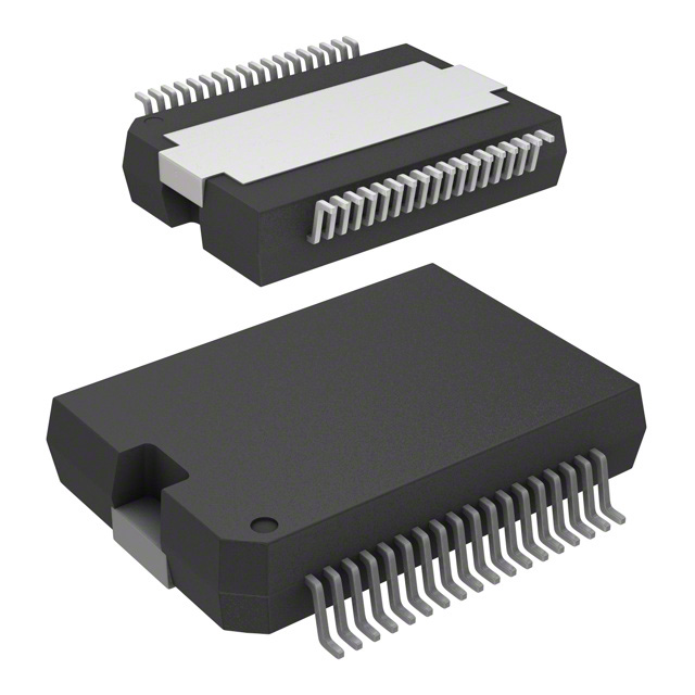
Infineon Technologies TLE8261EXUMA3
- Part No.:
- TLE8261EXUMA3
- Manufacturer:
- Infineon Technologies
- Category:
- Specialized ICs
- Package:
- 36-BSSOP (0.295", 7.50mm Width) Exposed Pad
- Datasheet:
-
 TLE8261EXUMA3.pdf
- Description:
- IC TRANSCEIVER DSO36-38
- Quantity:
- Payment:

- Shipping:

Inventory:1,674
Please send an inquiry. Send us your inquiry, and we will respond immediately.
Product details
Overview
TLE8261EXUMA3 from Infineon Technologies is a monolithic Universal System Basis Chip (SBC) for automotive CAN network nodes, integrating a high-speed CAN transceiver (ISO 11898-2/5 compliant), three LDO voltage regulators (Vcc1µC/Vcc2/Vcc3), SPI-configurable watchdog/reset supervision, wake-up input, and open-drain Limp Home output. It delivers 200 mA @ 5 V ±2% on Vcc1µC and Vcc2, supports up to 1 MBaud CAN data rate, and operates across −40 °C to +150 °C junction temperature.
For engineers reviewing the TLE8261EXUMA3 datasheet, TLE8261EXUMA3 pinout, TLE8261EXUMA3 application, or TLE8261EXUMA3 equivalent, key selection criteria include CAN bus fault tolerance (short-circuit proof to battery/GND), low-quiescent-current sleep mode (<30 µA), configurable watchdog timeout (16–1024 ms), and AEC-Q100 qualification for body control modules and gateway ECUs.
Technical Context
The TLE8261EXUMA3 implements a state-machine-driven SBC architecture with dedicated hardware blocks: a HS-CAN transceiver powered by VccHSCAN, dual 5 V LDOs (Vcc1µC and Vcc2) each rated 200 mA with ±2% accuracy, and a shunt-regulated Vcc3 output supporting up to 400 mA via external PNP transistor. All regulators feature overtemperature and short-circuit protection.
Supervision logic includes a window/watchdog timer configurable via 16-bit SPI, a reset output (RO) with integrated pull-up, and a bi-level wake-up input (WK) enabling cyclic wake in Stop Mode. The Limp Home output activates under critical failure (e.g., Vcc1µC undervoltage timeout) and is driven by dedicated internal logic supply for fail-safe operation.
Key Specifications
| Parameter | Value and Actual Design Meaning |
|---|---|
| CAN Data Rate | Up to 1 MBaud - enables real-time communication in high-speed automotive networks like body domain gateways. |
| Vcc1µC Output | 5 V ±2%, 200 mA - powers microcontrollers and RF receivers with tight regulation for stable digital operation. |
| Vcc2 Output | 5 V ±2%, 200 mA - supplies internal HS-CAN cell and external peripherals without cross-coupling risk. |
| Vcc3 Output | 5 V ±4%, up to 400 mA with 220 mΩ shunt + external PNP - flexible auxiliary supply for additional CAN transceivers or sensors. |
| Watchdog Timeout Range | 16 ms to 1024 ms, SPI-configurable - allows precise timing alignment with host MCU firmware execution cycles. |
| Quiescent Current (Sleep) | <30 µA - ensures battery longevity in always-on automotive modules such as door control units. |
| Operating Temperature | −40 °C to +150 °C (Tj) - meets under-hood thermal requirements for engine bay and transmission control applications. |
| ESD Robustness | 8 kV HBM on CANH/CANL/SPLIT - sustains field reliability in noisy vehicle environments without external protection. |
Pinout & Package
Package: PG-DSO-36-38 (exposed die pad), RoHS-compliant, AEC-Q100 qualified.
| Pin/Terminal | Circuit Role | Design Meaning |
|---|---|---|
| 1 RO | Reset Input/Output | Open-drain active-low reset signal with integrated pull-up; asserts system reset on Vcc1µC undervoltage or watchdog timeout. |
| 2 CSN | SPI Chip Select | Active-low enable for SPI communication; requires CLK to be low before assertion to prevent data corruption. |
| 3 CLK | SPI Clock Input | CMOS-level clock input with internal pull-down; synchronizes 16-bit SPI register reads/writes for configuration and status monitoring. |
| 4 SDI | SPI Data Input | Receives command bytes (e.g., watchdog setup, interrupt mask) from host MCU; validated against checksum for integrity. |
| 5 SDO | SPI Data Output | Transmits device status (e.g., CAN error flags, regulator faults, WK event latch) back to host MCU in real time. |
| 17 Vcc3shunt | Vcc3 Shunt Resistor Connection | Connects external 220 mΩ shunt to set current limit for Vcc3 output; enables scalable auxiliary power up to 400 mA. |
| 18 GND | Ground Reference | Primary analog/digital ground plane connection; multiple GND pins ensure low-impedance return paths for regulators and CAN bus. |
| 20 Vcc1µC | Microcontroller Supply Output | Stable 5 V ±2% regulated output delivering 200 mA; powers host MCU and associated logic with minimal ripple. |
| 21 Vcc3REF | Vcc3 Reference Voltage | Internal 5 V reference used to regulate Vcc3 via external PNP; decouples Vcc3 accuracy from shunt resistor tolerance. |
| 24 WK | Wake-Up Input | Bi-level sensitive input enabling wake from Sleep/Stop modes via CAN message, external signal, or SPI command. |
| 25 RxDCAN | CAN Receiver Data Input | Differential receiver input tied to CAN_L; complements TxDCAN for full-duplex HS-CAN communication per ISO 11898-2. |
| 26 TxDCAN | CAN Transmitter Data Output | Differential driver output tied to CAN_H; drives CAN_H/CAN_L bus pair with controlled slew rate for EMC compliance. |
| 27 n.c. | No Connect | Unbonded pin; must remain unconnected to avoid parasitic coupling or ESD path disruption. |
| 28 Limp home | Limp Home Output | Open-drain safety output activated during critical failures (e.g., Vcc1µC UVLO); drives external fail-safe circuitry. |
| 29 INT | Interrupt Output | Active-low push-pull interrupt signal indicating events like WK detection, CAN error, or regulator fault; filterable to prevent chatter. |
| 30 Vs | Main Supply Input | Battery-supplied input (5.5–28 V); powers internal regulators and CAN transceiver; includes reverse-polarity and load-dump protection. |
| 31 Vcc2 | Secondary Regulator Output | 5 V ±2%, 200 mA output dedicated to internal HS-CAN cell and optional external peripherals; isolated from Vcc1µC domain. |
| 32 VccHSCAN | CAN Transceiver Supply | Dedicated 5 V supply input for HS-CAN transceiver; enables independent power cycling and fault containment. |
| 33 SPLIT | CAN Common-Mode Stabilization | Connects to center-tap of common-mode choke; reduces electromagnetic emissions and improves bus immunity per ISO 11898-2. |
| 34 CANL | CAN Low Bus Line | Differential CAN bus line referenced to GND; short-circuit proof to battery and GND; supports bus wake-up detection. |
| 35 CANH | CAN High Bus Line | Differential CAN bus line referenced to GND; short-circuit proof to battery and GND; supports bus wake-up detection. |
| 36 Test | Development Mode Enable | Enables SBC SW Development Mode when pulled high; disables watchdog reset assertion for debug sessions. |
Key Features
| Feature | Design Value |
|---|---|
| Integrated HS-CAN Transceiver | Fully compliant with ISO 11898-2 and ISO 11898-5; supports 1 MBaud with bus wake-up, failure detection, and ±8 kV ESD robustness. |
| Dual Independent 5 V LDOs | Vcc1µC and Vcc2 each deliver 200 mA at ±2% accuracy; electrically isolated to prevent fault propagation between MCU and CAN domains. |
| Configurable Window Watchdog | SPI-programmable timeout (16–1024 ms) with checksum-protected configuration; reset inhibition via Test pin for development. |
| Limp Home Fail-Safe Output | Open-drain output driven by dedicated internal logic supply; activates on Vcc1µC undervoltage timeout or critical fault for safe degradation. |
| Bi-Level Wake-Up Input (WK) | Detects both rising and falling edges; enables wake from ultra-low-power Stop Mode without external components or polling overhead. |
| Low-Power Sleep Mode | Quiescent current <30 µA with all regulators active; maintains CAN bus monitoring and WK sensitivity while minimizing battery drain. |
Applications
| Body Control Module (BCM) | Door Control Unit (DCU) |
|---|---|
|
Use Scenario: Centralized management of lighting, windows, locks, and mirrors in passenger vehicles. IC Role / Device Role / Timing Role: System Basis Chip providing regulated power (Vcc1µC/Vcc2), HS-CAN interface, and fail-safe Limp Home output for degraded operation. Use Value: Eliminates need for discrete regulators and CAN transceivers; reduces BOM count by 4+ components while meeting AEC-Q100 Class 0 requirements. |
Use Scenario: Localized control of power windows, central locking, and mirror adjustment in each vehicle door. IC Role / Device Role / Timing Role: Power management and communication hub with bi-level WK input enabling instant wake from sleep upon door handle touch or key fob signal. Use Value: Achieves <30 µA quiescent current in sleep mode, extending battery life in always-connected modules without compromising responsiveness. |
| Gateway ECU | Roof Control Module |
|
Use Scenario: Bridging CAN FD, LIN, and Ethernet domains in modern vehicle architectures. IC Role / Device Role / Timing Role: HS-CAN node with SPI-configurable watchdog and interrupt-driven status reporting for real-time diagnostics and firmware updates. Use Value: Enables deterministic watchdog timeouts aligned to gateway boot sequence; SPI interface allows dynamic reconfiguration without hardware change. |
Use Scenario: Managing sunroof, ambient lighting, and HVAC controls mounted in vehicle roof console. IC Role / Device Role / Timing Role: Compact power and communication solution with exposed-pad DSO-36 package optimized for space-constrained PCB layouts. Use Value: Thermal resistance reduced by 35% vs. standard SOIC due to exposed die pad, sustaining 150 °C junction temperature in enclosed roof environments. |
Equivalent & Alternatives
The following parts are listed as comparable options for similar system basis chip applications.
| Alternative Part | Technical Difference | Application Difference | Selection Advice |
|---|---|---|---|
| NXP MC33816 | Single 5 V LDO (250 mA), no Vcc3 shunt option; integrated LIN physical layer (absent in TLE8261EXUMA3). | Targeted at LIN-centric body nodes; lacks Vcc3 flexibility for multi-transceiver CAN designs. | Select when LIN interface is mandatory and auxiliary power scalability is not required. |
| Renesas RAA270020 | Supports CAN FD (5 Mbps), includes embedded EEPROM for configuration storage; higher quiescent current (55 µA in sleep mode). | Suitable for next-gen gateways requiring CAN FD bandwidth and non-volatile settings retention. | Select when future-proofing for CAN FD or eliminating external EEPROM is prioritized over ultra-low sleep current. |
Compared with MC33816 and RAA270020, the TLE8261EXUMA3 uniquely balances triple-LDO flexibility, sub-30 µA sleep current, and proven AEC-Q100 reliability for cost-sensitive CAN-only body electronics-without adding LIN or CAN FD complexity.
Availability
TLE8261EXUMA3 is available at Aetrix Electronics and suitable for body control modules, door control units, gateway ECUs, and roof control modules requiring stable component supply across automotive production lifecycles.
Supply support for TLE8261EXUMA3 includes scheduled delivery planning, volume procurement assistance, BOM continuity management, traceable sourcing, and lifecycle availability coordination for OEM customers, industrial embedded developers, connected-device designers, and electronics production programs.
Manufacturer
Infineon Technologies is a German semiconductor manufacturer specializing in power management, automotive ICs, and security solutions, with global manufacturing and automotive qualification expertise.
The TLE8261EXUMA3 belongs to the HERMES family of System Basis Chips designed specifically for CAN-based automotive electronic control units requiring integrated power, communication, and safety supervision in harsh environments.
FAQ
What is the maximum allowable input voltage on the Vs pin?
The Vs pin accepts 5.5 V to 28 V DC, with absolute maximum rating of 40 V for transient load dump conditions per ISO 7637-2 Pulse 5a. Internal protection circuitry clamps voltage above 34 V and limits energy dissipation to prevent damage during automotive load dump events.
Can the Limp Home output drive an external relay directly?
No-the Limp Home pin is an open-drain output rated for 100 mA sink current at 5 V. It requires an external pull-up to Vcc1µC or Vcc2 and a driver stage (e.g., NPN transistor or MOSFET) to energize relays or high-current loads; direct relay connection risks exceeding safe operating area.
How is CAN bus wake-up detected in Sleep Mode?
In Sleep Mode, the HS-CAN transceiver remains partially active and monitors differential voltage on CANH/CANL. A dominant bit (CANH > CANL by ≥0.9 V) lasting ≥120 ns triggers wake-up, asserting the WK signal internally and transitioning the SBC to Standby Mode within 10 µs.
Does the SPI interface support daisy-chaining multiple TLE8261EXUMA3 devices?
No-each TLE8261EXUMA3 requires a dedicated CSN line; the SPI is point-to-point only. Daisy-chaining is unsupported due to lack of SPI output-enable control on SDO and absence of hardware address decoding in the protocol stack.
TLE8261EXUMA3 Specifications
- Product attributes
- Attribute value
- Manufacturer:
- Infineon Technologies
- Series:
- -
- Package/Case:
- 36-BSSOP (0.295", 7.50mm Width) Exposed Pad
- Packaging:
- Tape & Reel (TR)
- Product Status:
- Obsolete
- Programmable:
- Not Verified
- Type:
- Transceiver
- Applications:
- -
- Mounting Type:
- Surface Mount
- Supplier Device Package:
- PG-DSO-36-38
- Grade:
- Automotive
- Qualification:
- -
TLE8261EXUMA3 FAQ
1.How can I place an order for TLE8261EXUMA3 through Aetrix?
Please submit a Request for Quotation (RFQ) for TLE8261EXUMA3 on Aetrix. Our sales agent will provide a competitive quotation and guide you through the order confirmation once you accept the terms.
2.Are the price and stock information for TLE8261EXUMA3 reliable?
The price and inventory of TLE8261EXUMA3 are updated periodically and may fluctuate due to market conditions. Stock and pricing data are typically refreshed every 24 hours. Quotation validity for TLE8261EXUMA3 is usually 5 days.
3.What payment methods are accepted for TLE8261EXUMA3?
We accept Wire Transfer, PayPal, Credit Card, Western Union, MoneyGram, and Escrow for TLE8261EXUMA3 transactions.
Note: Certain payment methods may incur a processing fee.
4.How is shipping managed for TLE8261EXUMA3?
TLE8261EXUMA3 orders can be shipped via leading logistics carriers, including DHL, UPS, FedEx, TNT, or Registered Mail.
Once your TLE8261EXUMA3 order is processed, you will receive an email with the shipment details and tracking number.
Note: Tracking information may take up to 24 hours to appear. Express delivery typically takes 3–5 business days.
5.How can I obtain technical support or documentation for TLE8261EXUMA3?
For technical support, including TLE8261EXUMA3 datasheets, pinout diagrams, or application guidance, please contact our engineering support team. They can provide detailed documentation and assistance for your TLE8261EXUMA3 requirements.
6.How does Aetrix verify that TLE8261EXUMA3 is sourced from the original manufacturer or authorized distributors?
All TLE8261EXUMA3 products on Aetrix are procured from qualified distributors and authorized channels. Our dedicated quality assurance team conducts strict verification, including traceability checks and, if necessary, third-party testing. This ensures that TLE8261EXUMA3 meets industry standards.
7.What is the process for return or replacement of TLE8261EXUMA3?
All TLE8261EXUMA3 units undergo pre-shipment inspection (PSI). If there is an issue with TLE8261EXUMA3, returns or replacements are accepted under the following conditions:
1.Quantity discrepancies, incorrect items, or visible external defects (such as breakage or corrosion), acknowledged by Aetrix.
2.The issue is reported within 90 days of delivery.
3.The TLE8261EXUMA3 part is unused and in its original packaging.
Return procedure for TLE8261EXUMA3:
1.Submit a request within 90 days.
2.Obtain a Return Material Authorization (RMA) from Aetrix.
TLE8261EXUMA3 Tags

-
CAP200DG-TL
Power Integrations
-
ATSHA204A-MAHDA-T
Microchip Technology

-
ATSHA204A-SSHDA-T
Microchip Technology

-
ATSHA204A-STUCZ-T
Microchip Technology
-
ATECC608B-MAHDA-T
Microchip Technology
-
ATECC608B-MAHCZ-S
Microchip Technology

-
ATECC608B-SSHDA-T
Microchip Technology
-
ATECC608B-MAHDA-S
Microchip Technology
-
ATECC608A-MAHDA-S
Microchip Technology
-
ATECC608B-MAVDA-T
Microchip Technology

-
ATECC608A-SSHDA-T
Microchip Technology
-
ATECC508A-MAHDA-T
Microchip Technology
Tech Hub

Jumper cables guide covering safe connection order, red and black clamp placement, final ground connection, cable gauge, length, clamp quality, copper vs CCA cables, jump starter comparison and battery…

LDO regulator guide covering low dropout voltage, power dissipation, thermal design, PSRR, output noise, capacitor stability, adjustable LDO circuits, LDO vs buck converter and datasheet selection chec…

Conditional Access Module guide covering CAM meaning, CI/CI+ interface, smart card authorization, DVB security workflow, TV and set-top box compatibility, internal electronics, ESD protection, connecto…

Guide to electronic component obsolescence covering EOL risk, PCN/PDN notices, last-time buy planning, replacement options, form-fit-function validation, counterfeit risk and BOM lifecycle management.

18650 battery guide covering lithium-ion cell basics, 3.6V/3.7V voltage, 4.2V charging, mAh and Wh capacity, protected cells, chargers, BMS, series-parallel packs, holders, welding and sourcing checks.…

Hall effect sensor guide covering working principle, linear and digital sensors, Arduino circuits, current sensing, speed detection, automotive applications, A3144 examples, signal filtering and datash…

Product Change Notification guide for electronic components, covering PCN meaning, PCN vs PDN/EOL, common change types, risk levels, form-fit-function review, engineering validation, BOM control, LTB/L…

A practical guide to blend door actuators, covering HVAC function, symptoms, location, AC and heater issues, reset and calibration, replacement cost, electrical diagnosis, compatibility checks, and rep…

Engineering guide to Raspberry Pi alternatives, covering chip-level differences, Orange Pi, ROCK, Jetson, Banana Pi, NanoPi, Compute Module, Pico, GPIO, camera, HAT compatibility, and replacement risks…

Engineering guide to dynamic load response testing for high-current buck converters, covering load step setup, slew rate, Vcore undershoot, overshoot, recovery time, probe location, output capacitors a…


