
 My Inquiry
 My Account


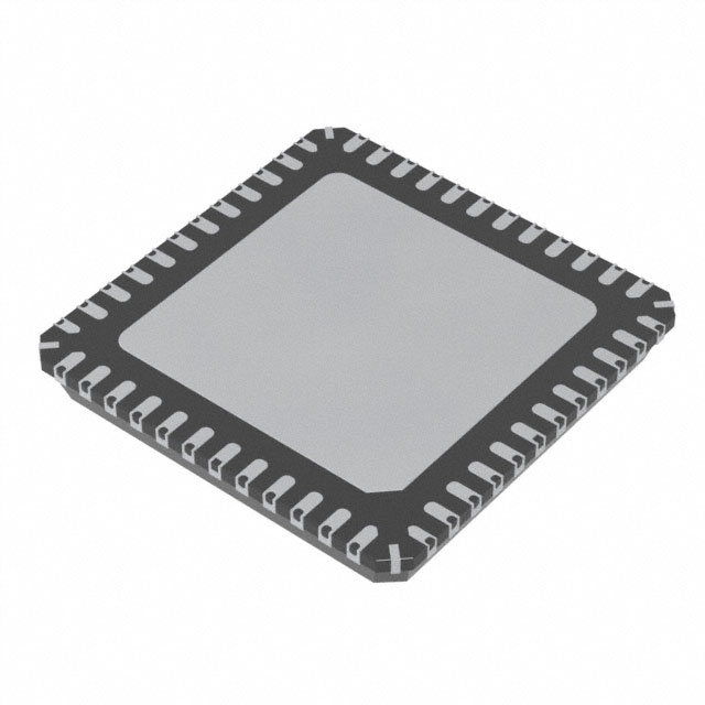
Infineon Technologies TLE9262QXV33XUMA1
- Part No.:
- TLE9262QXV33XUMA1
- Manufacturer:
- Infineon Technologies
- Category:
- Specialized
- Package:
- 48-VFQFN Exposed Pad
- Datasheet:
-
 TLE9262QXV33XUMA1.pdf
- Description:
- IC INTERFACE SPECIALIZED 48VQFN
- Quantity:
- Payment:

- Shipping:

Inventory:4,408
Please send an inquiry. Send us your inquiry, and we will respond immediately.
Product details
Overview
TLE9262QXV33XUMA1 from Infineon Technologies is a 48-pin automotive-grade system basis chip (SBC) integrating a 3.3 V/250 mA LDO, high-side and low-side switch drivers, watchdog timer, and SPI interface for microcontroller power management and communication in 12 V/48 V dual-battery vehicle architectures. It supports CAN FD physical layer compliance and operates over -40 °C to 150 °C ambient temperature.
For engineers reviewing the TLE9262QXV33XUMA1 datasheet, TLE9262QXV33XUMA1 pinout, TLE9262QXV33XUMA1 application, or TLE9262QXV33XUMA1 equivalent, key selection criteria include integrated 3.3 V LDO output capability, dual-battery voltage monitoring thresholds (VBAT1/VBAT2), programmable watchdog timeout, SPI register access for diagnostics, and AEC-Q100 Grade 0 qualification.
Technical Context
The TLE9262QXV33XUMA1 implements a multi-rail power management architecture with independent high-side (HS1/HS2) and low-side (LS1/LS2) drivers capable of 600 mA continuous load current each, supporting wake-up via CAN bus or external pins. Its embedded watchdog features windowed timeout and reset generation on SPI command failure or clock fault detection.
Integrated analog comparators monitor VBAT1 (12 V system) and VBAT2 (48 V system) with programmable undervoltage/overvoltage thresholds and hysteresis. The 3.3 V LDO supplies microcontroller core logic with ±2 % output accuracy and short-circuit protection.
Key Specifications
| Parameter | Value and Actual Design Meaning |
|---|---|
| LDO Output | 3.3 V ±2 %, 250 mA max - powers MCU core logic with tight regulation and thermal foldback |
| High-Side Drivers | 2× HS outputs, 600 mA continuous, 1.2 A peak - drives external MOSFETs for battery domain switching |
| Low-Side Drivers | 2× LS outputs, 600 mA continuous, 1.2 A peak - controls ground-referenced loads like sensors or LEDs |
| Watchdog Type | Windowed watchdog with SPI-triggered refresh - prevents runaway firmware by requiring periodic valid SPI commands |
| Operating Temp | -40 °C to +150 °C ambient - qualified for engine bay and transmission control unit placement |
| CAN FD Support | Compatible with ISO 11898-2:2016 physical layer - enables high-speed communication up to 5 Mbit/s in next-gen EVs |
| AEC-Q100 Grade | Grade 0 (−40 °C to +150 °C) - meets stringent automotive reliability requirements for safety-critical ECUs |
Pinout & Package
48-pin QFN package (7 mm × 7 mm, 0.5 mm pitch) with exposed thermal pad; RoHS-compliant, lead-free, and halogen-free.
| Pin/Terminal | Circuit Role | Design Meaning |
|---|---|---|
| VDDIO | I/O supply input | Provides 3.3 V to SPI interface and digital logic; decoupling required at pin |
| VCC | Main supply input | Accepts 5.5–28 V for internal regulators and driver stages; connects to 12 V battery rail |
| VCC2 | Secondary supply input | Accepts 16–58 V for 48 V domain monitoring and HS/LS driver operation |
| VSUP | Supply sense input | Monitors VCC voltage for undervoltage lockout and brownout detection |
| WDI | Watchdog input | External reset trigger; falling edge initiates watchdog window restart |
| SPI_CS | SPI chip select | Active-low enable for SPI register access; synchronous with SCLK and MOSI/MISO |
Key Features
| Feature | Design Value |
|---|---|
| Dual-battery monitoring | Independent VBAT1 (12 V) and VBAT2 (48 V) comparators with programmable UV/OV thresholds and hysteresis |
| Programmable watchdog | Configurable window timeout (1 ms–10 s) and SPI-based refresh; failsafe reset on invalid command or clock loss |
| Thermal protection | Internal die temperature sensing with automatic shutdown at >175 °C and hysteresis-based recovery |
| SPI diagnostic interface | 16-bit register map for real-time readout of supply voltages, temperature, driver status, and fault flags |
| Wake-up sources | Three independent wake-up inputs (WAKE1–WAKE3) plus CAN bus activity detection for low-power sleep mode exit |
Applications
| Engine Control Unit (ECU) | 48 V Mild Hybrid Powertrain |
|---|---|
Use Scenario: Central power management and MCU supervision in gasoline/diesel engine control modules. IC Role / Device Role / Timing Role: System basis chip providing regulated 3.3 V supply, watchdog supervision, and CAN FD interface for main MCU. Use Value: Enables fail-safe operation during cranking transients and ensures deterministic reset behavior under voltage dips below 6 V. | Use Scenario: Power domain control and diagnostics in 48 V belt-driven starter generators (BSG) and P0/P1 hybrid architectures. IC Role / Device Role / Timing Role: Dual-rail supervisor managing both 12 V infotainment and 48 V propulsion subsystems with coordinated wake-up and fault reporting. Use Value: Reduces BOM count by consolidating discrete LDOs, watchdog ICs, and switch drivers while maintaining ASIL-B compliance. |
| Electric Power Steering (EPS) | Brake-by-Wire Actuator |
Use Scenario: Safety-critical motor control module requiring redundant power supervision and fast fault response. IC Role / Device Role / Timing Role: Primary SBC delivering 3.3 V MCU supply, HS/LS driver control for torque motor H-bridge, and SPI-linked diagnostics. Use Value: Supports functional safety requirements (ISO 26262 ASIL-B) via hardware-based watchdog and supply monitoring with <10 µs fault detection latency. | Use Scenario: Electro-hydraulic brake actuation system demanding high reliability and precise voltage domain isolation. IC Role / Device Role / Timing Role: Dual-supply supervisor enabling independent 12 V control logic and 48 V solenoid drive power paths with cross-domain fault signaling. Use Value: Eliminates need for separate 48 V monitor ICs and reduces PCB area by 35% versus discrete solution. |
Equivalent & Alternatives
The following parts are listed as comparable options for similar system basis chip applications.
| Alternative Part | Technical Difference | Application Difference | Selection Advice |
|---|---|---|---|
| TLE9263QXV33XUMA1 | Same pinout and feature set but adds LIN transceiver and enhanced ESD protection (±8 kV HBM) | Required where LIN communication coexists with CAN FD in body control modules | Select when LIN physical layer integration is needed without adding discrete transceiver |
| MC33FS4500A5ES | Offers 5 V LDO instead of 3.3 V; lacks 48 V monitoring; supports SENT sensor interface | Better suited for legacy 5 V MCU platforms without 48 V architecture requirements | Prefer for non-hybrid vehicles using 5 V microcontrollers and analog sensor interfaces |
Compared with TLE9262QXV33XUMA1, the TLE9263 variant adds LIN capability at no pinout cost, while the MC33FS4500 targets 5 V systems without 48 V support-making the TLE9262 optimal for new 48 V mild hybrid designs needing 3.3 V MCU supply and dual-battery monitoring.
Availability
TLE9262QXV33XUMA1 is available at Aetrix Electronics and suitable for engine control units, 48 V mild hybrid powertrains, electric power steering modules, and brake-by-wire actuators requiring stable component supply across automotive production lifecycles.
Supply support for TLE9262QXV33XUMA1 includes scheduled delivery planning, volume procurement assistance, BOM continuity management, traceable sourcing, and lifecycle availability coordination for OEM customers, industrial embedded developers, connected-device designers, and electronics production programs.
Manufacturer
Infineon Technologies is a German semiconductor manufacturer specializing in power management, automotive ICs, and security solutions, with global R&D and manufacturing infrastructure.
The TLE9262 belongs to Infineon's Automotive System Basis Chip (SBC) product line, designed specifically for centralized power management, communication interface support, and functional safety compliance in modern 12 V/48 V vehicle electrical architectures.
FAQ
What is the maximum allowable voltage on the VCC2 pin?
The VCC2 pin accepts 16 V to 58 V DC, supporting direct connection to 48 V battery rails. Absolute maximum rating is 60 V for transient spikes per ISO 7637-2 Pulse 5a. Operation above 58 V risks permanent damage to internal high-voltage circuitry and voids AEC-Q100 qualification.
Does the TLE9262QXV33XUMA1 support SPI clock frequencies above 10 MHz?
Yes, the SPI interface supports up to 20 MHz clock frequency with standard mode timing. At 20 MHz, setup/hold times remain within specification for all operating temperatures (−40 °C to +150 °C), enabling fast register reads during runtime diagnostics without compromising data integrity.
Can the watchdog be disabled after power-on reset?
No-the watchdog is enabled by default after POR and cannot be permanently disabled via SPI. It can only be temporarily suspended for ≤100 ms using the WDI pin, ensuring continuous supervision even if firmware becomes unresponsive or loses SPI communication.
Is the thermal pad on the QFN package electrically connected?
Yes, the exposed thermal pad is internally connected to GND and must be soldered to a PCB thermal land tied to the main ground plane. Failure to connect it results in degraded thermal performance, exceeding 150 °C junction temperature under full load and triggering premature thermal shutdown.
TLE9262QXV33XUMA1 Specifications
- Product attributes
- Attribute value
- Manufacturer:
- Infineon Technologies
- Series:
- -
- Package/Case:
- 48-VFQFN Exposed Pad
- Packaging:
- Tape & Reel (TR)
- Product Status:
- Obsolete
- Applications:
- -
- Interface:
- SPI
- Voltage - Supply:
- 28V
- Supplier Device Package:
- PG-VQFN-48-31
- Grade:
- Automotive
- Qualification:
- -
- Mounting Type:
- Surface Mount
TLE9262QXV33XUMA1 FAQ
1.How can I place an order for TLE9262QXV33XUMA1 through Aetrix?
Please submit a Request for Quotation (RFQ) for TLE9262QXV33XUMA1 on Aetrix. Our sales agent will provide a competitive quotation and guide you through the order confirmation once you accept the terms.
2.Are the price and stock information for TLE9262QXV33XUMA1 reliable?
The price and inventory of TLE9262QXV33XUMA1 are updated periodically and may fluctuate due to market conditions. Stock and pricing data are typically refreshed every 24 hours. Quotation validity for TLE9262QXV33XUMA1 is usually 5 days.
3.What payment methods are accepted for TLE9262QXV33XUMA1?
We accept Wire Transfer, PayPal, Credit Card, Western Union, MoneyGram, and Escrow for TLE9262QXV33XUMA1 transactions.
Note: Certain payment methods may incur a processing fee.
4.How is shipping managed for TLE9262QXV33XUMA1?
TLE9262QXV33XUMA1 orders can be shipped via leading logistics carriers, including DHL, UPS, FedEx, TNT, or Registered Mail.
Once your TLE9262QXV33XUMA1 order is processed, you will receive an email with the shipment details and tracking number.
Note: Tracking information may take up to 24 hours to appear. Express delivery typically takes 3–5 business days.
5.How can I obtain technical support or documentation for TLE9262QXV33XUMA1?
For technical support, including TLE9262QXV33XUMA1 datasheets, pinout diagrams, or application guidance, please contact our engineering support team. They can provide detailed documentation and assistance for your TLE9262QXV33XUMA1 requirements.
6.How does Aetrix verify that TLE9262QXV33XUMA1 is sourced from the original manufacturer or authorized distributors?
All TLE9262QXV33XUMA1 products on Aetrix are procured from qualified distributors and authorized channels. Our dedicated quality assurance team conducts strict verification, including traceability checks and, if necessary, third-party testing. This ensures that TLE9262QXV33XUMA1 meets industry standards.
7.What is the process for return or replacement of TLE9262QXV33XUMA1?
All TLE9262QXV33XUMA1 units undergo pre-shipment inspection (PSI). If there is an issue with TLE9262QXV33XUMA1, returns or replacements are accepted under the following conditions:
1.Quantity discrepancies, incorrect items, or visible external defects (such as breakage or corrosion), acknowledged by Aetrix.
2.The issue is reported within 90 days of delivery.
3.The TLE9262QXV33XUMA1 part is unused and in its original packaging.
Return procedure for TLE9262QXV33XUMA1:
1.Submit a request within 90 days.
2.Obtain a Return Material Authorization (RMA) from Aetrix.
TLE9262QXV33XUMA1 Tags

-
NVT4857UKAZ
NXP USA Inc.

-
TCA8418RTWR
Texas Instruments

-
PCA9546APWR
Texas Instruments

-
MD0100N8-G
Microchip Technology

-
PCA9548APW,118
NXP USA Inc.

-
PCA9540BDP,118
NXP USA Inc.

-
PCA9548APWR
Texas Instruments

-
PCA9546APW,118
NXP USA Inc.

-
PTN3360DBS,518
NXP USA Inc.

-
PCA9546ABS,118
NXP USA Inc.

-
PCA9518PWR
Texas Instruments

-
PCA9545APW,118
NXP USA Inc.
Tech Hub

An engineering guide to LED driver operation, constant-current and constant-voltage outputs, linear and switching topologies, dimming, IC selection, calculations, replacement compatibility, and fault c…

Operational amplifier guide covering op amp basics, feedback, ideal vs real op amps, common configurations, buffer circuits, offset, bias current, gain-bandwidth, slew rate, rail-to-rail limits and sel…

Jumper cables guide covering safe connection order, red and black clamp placement, final ground connection, cable gauge, length, clamp quality, copper vs CCA cables, jump starter comparison and battery…

LDO regulator guide covering low dropout voltage, power dissipation, thermal design, PSRR, output noise, capacitor stability, adjustable LDO circuits, LDO vs buck converter and datasheet selection chec…

Conditional Access Module guide covering CAM meaning, CI/CI+ interface, smart card authorization, DVB security workflow, TV and set-top box compatibility, internal electronics, ESD protection, connecto…

Guide to electronic component obsolescence covering EOL risk, PCN/PDN notices, last-time buy planning, replacement options, form-fit-function validation, counterfeit risk and BOM lifecycle management.

18650 battery guide covering lithium-ion cell basics, 3.6V/3.7V voltage, 4.2V charging, mAh and Wh capacity, protected cells, chargers, BMS, series-parallel packs, holders, welding and sourcing checks.…

Hall effect sensor guide covering working principle, linear and digital sensors, Arduino circuits, current sensing, speed detection, automotive applications, A3144 examples, signal filtering and datash…

Product Change Notification guide for electronic components, covering PCN meaning, PCN vs PDN/EOL, common change types, risk levels, form-fit-function review, engineering validation, BOM control, LTB/L…

A practical guide to blend door actuators, covering HVAC function, symptoms, location, AC and heater issues, reset and calibration, replacement cost, electrical diagnosis, compatibility checks, and rep…


