
 My Inquiry
 My Account


Infineon Technologies TLE9262QXXUMA2
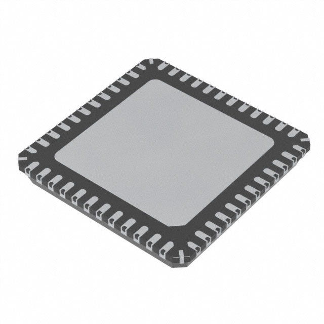
- Part No.:
- TLE9262QXXUMA2
- Manufacturer:
- Infineon Technologies
- Category:
- Specialized
- Package:
- 48-VFQFN Exposed Pad
- Datasheet:
-
 TLE9262QXXUMA2.pdf
- Description:
- IC INTERFACE SPECIALIZED 48VQFN
- Quantity:
- Payment:

- Shipping:

Inventory:1,776
Please send an inquiry. Send us your inquiry, and we will respond immediately.
Product details
Overview
TLE9262QXXUMA2 from Infineon Technologies is an automotive System Basis Chip (SBC) integrating dual low-dropout voltage regulators (5.0 V/150 mA and 3.3 V/50 mA), HS-CAN transceiver supporting CAN FD, LIN transceiver, four high-side switches (HS1–HS4), two high-voltage wake inputs (WK1/WK2), watchdog, reset, and fail-safe supervision. It serves as central power management and communication interface in body control modules for 12 V vehicle electrical systems.
For engineers reviewing the TLE9262QXXUMA2 datasheet, TLE9262QXXUMA2 pinout, TLE9262QXXUMA2 application, or TLE9262QXXUMA2 equivalent, key selection criteria include CAN FD/LIN co-integration, dual LDO output stability under load transients, high-side switch current limiting (1.8 A typ.), wake input voltage tolerance (up to 28 V), and fail-safe state machine behavior across SBC modes (Normal, Stop, Sleep, Fail-Safe).
Technical Context
This SBC implements a deterministic finite-state machine with seven operational modes (Init, Normal, Stop, Sleep, Restart, Fail-Safe, Development), each governing regulator enablement, transceiver activity, switch control, and wake response. The CAN transceiver supports dominant timeout, bus clamping, and wake detection compliant with ISO 11898-2:2013 and CAN FD physical layer requirements.
The LIN transceiver meets ISO 17987-2/ISO 17987-4 specifications, including flash programming via LIN, slope selection for EMI reduction, and receive-only mode for diagnostics. Voltage supervision includes independent monitoring of VCC, VS, and external regulator feedback, triggering reset or fail outputs on violation.
Key Specifications
| Parameter | Value and Actual Design Meaning |
|---|---|
| VREG1 Output | 5.0 V ±2%, 150 mA max - powers microcontroller core logic and CAN/LIN PHYs |
| VREG2 Output | 3.3 V ±2%, 50 mA max - supplies MCU I/O banks and sensor interfaces |
| CAN Bus Voltage Range | ±40 V common-mode, 2.2 V differential threshold - enables robust operation in noisy 12 V automotive environments |
| LIN Bus Voltage Range | 8 V to 18 V supply, ±40 V fault tolerance - supports direct battery connection without external protection |
| High-Side Switch RDS(on) | 120 mΩ typ. at 25°C - limits power loss and thermal rise during 1.8 A continuous load switching |
| Wake Input Threshold | WK1/WK2: 4.5 V to 28 V detection range with hysteresis - enables reliable wake from deep sleep using door handle or PKE signals |
| Watchdog Timeout | Configurable 1.6 ms to 2.1 s window - ensures MCU firmware liveness without requiring external timing components |
Pinout & Package
Package: PG-VQFN-48-19 (4.0 mm × 4.0 mm, 0.4 mm pitch, exposed thermal pad). Pin count: 48 terminals. Pin functions validated per Infineon TLE9262QX Data Sheet Rev. 1.1 (2014-09-26), Sections 3.1–3.2.
| Pin/Terminal | Circuit Role | Design Meaning |
|---|---|---|
| VCC | Main supply input | 12 V system rail input; powers internal regulators and logic; requires 10 µF ceramic decoupling |
| VS | Battery sense input | Direct connection to battery for undervoltage/overvoltage monitoring and wake source |
| HS1–HS4 | High-side switch outputs | Four independently controlled NMOS drivers; each supports open-load detection and PWM dimming |
| WK1, WK2 | High-voltage wake inputs | 28 V tolerant digital inputs; configurable as wake sources or analog measurement channels (0–5 V) |
| CANH, CANL | CAN differential bus interface | Integrated termination and bus fault protection; supports CAN FD data rates up to 5 Mbit/s |
| LIN | LIN single-wire bus interface | Bi-directional half-duplex node; integrated pull-up, slew rate control, and short-to-battery protection |
| RESET | Reset output | Active-low open-drain signal; asserts during VCC/VREG faults or watchdog timeout |
| FO1–FO3 | Fail outputs | Dedicated diagnostic outputs indicating SBC failure states (e.g., overtemperature, regulator fault) |
Key Features
| Feature | Design Value |
|---|---|
| Integrated CAN FD + LIN Transceivers | Eliminates need for discrete transceivers; reduces BOM count and PCB area while ensuring protocol-compliant timing and fault handling |
| Dual Independent LDO Regulators | Enables simultaneous powering of 5 V MCU core and 3.3 V peripherals with separate enable/control and independent fault reporting |
| Programmable High-Side Switches | Each HSx supports current limiting, open-load detection, and PWM-controlled duty cycle-ideal for LED lighting and solenoid actuation |
| Multi-Mode State Machine | Hardware-enforced transitions between Normal, Stop, Sleep, and Fail-Safe modes reduce software complexity and improve ASIL-B compliance |
| Wake Input Dual Functionality | WK1/WK2 serve as either wake triggers or analog measurement inputs (10-bit resolution), increasing system flexibility without added ADC pins |
Applications
| Body Control Module (BCM) | Door Control Unit (DCU) |
|---|---|
Use Scenario: Centralized power and communication hub managing interior lighting, window lifts, mirror controls, and door lock actuators in modern vehicles. IC Role / Device Role / Timing Role: System Basis Chip providing regulated power, CAN FD backbone connectivity, LIN sub-network control, and local high-side drive for loads. Use Value: Reduces component count by consolidating regulators, transceivers, and switches into one AEC-Q100 qualified device, lowering system cost and improving reliability. |
Use Scenario: Local controller inside vehicle door assemblies handling window motor, lock solenoid, mirror position, and anti-pinch sensing. IC Role / Device Role / Timing Role: Power manager and LIN node enabling distributed intelligence; wake inputs detect door handle touch or key fob proximity. Use Value: Enables ultra-low-power sleep (<15 µA) with fast wake response (<100 µs), extending battery life in keyless entry systems. |
| Roof Module Control | Seat Control Unit |
Use Scenario: Managing sunroof motor, ambient lighting, and rain sensor interface in roof console assemblies. IC Role / Device Role / Timing Role: High-side switch driver for bidirectional DC motors and analog input conditioner for capacitive rain sensors. Use Value: Integrated open-load detection prevents false motor stall alarms; cyclic wake capability supports periodic sensor polling without MCU intervention. |
Use Scenario: Controlling seat position motors, heating elements, and memory function EEPROM via LIN in premium seating systems. IC Role / Device Role / Timing Role: LIN master node with embedded flash programming support, allowing field updates of seat profile configurations. Use Value: Flash programming via LIN eliminates need for dedicated programming headers, simplifying assembly and service workflows. |
Equivalent & Alternatives
The following parts are listed as comparable options for similar automotive SBC applications.
| Alternative Part | Technical Difference | Application Difference | Selection Advice |
|---|---|---|---|
| NXP MC33903 | Single 5 V LDO (250 mA), no integrated LIN transceiver, CAN only (non-FD), 3 high-side switches | Lacks CAN FD and LIN integration; requires external LIN transceiver for LIN nodes | Select when CAN FD and LIN co-integration are not required and higher LDO current is needed |
| Renesas ISL78228 | Dual buck regulators (3.3 V/2 A, 5.0 V/1.5 A), no CAN/LIN, no high-side switches, automotive grade | Pure power management IC; lacks communication and load driving functions entirely | Select when system uses separate communication ICs and discrete high-side drivers |
Compared with MC33903 and ISL78228, TLE9262QXXUMA2 uniquely integrates CAN FD, LIN, dual LDOs, and four high-side switches in a single AEC-Q100 Grade 1 package-reducing interconnect complexity and enabling compact, functionally complete body domain controllers.
Availability
TLE9262QXXUMA2 is available at Aetrix Electronics and suitable for body control modules, door control units, roof modules, and seat control units requiring stable component supply, automotive qualification, and long-term lifecycle support.
Supply support for TLE9262QXXUMA2 includes scheduled delivery planning, volume procurement assistance, BOM continuity management, traceable sourcing, and lifecycle availability coordination for OEM customers, industrial embedded developers, connected-device designers, and electronics production programs.
Manufacturer
Infineon Technologies is a German semiconductor manufacturer specializing in power management, automotive electronics, and security solutions, with global manufacturing and R&D infrastructure.
The TLE9262QXXUMA2 belongs to Infineon's TLE926x mid-range System Basis Chip family, designed specifically for cost-optimized, ASIL-B capable body electronics applications requiring integrated power, communication, and load driving in compact packages.
FAQ
What is the maximum allowable junction temperature for continuous operation?
The TLE9262QXXUMA2 has a maximum junction temperature of +150 °C, validated per AEC-Q100 stress test conditions. Thermal design must maintain θJA ≤ 45 K/W in typical PCB layouts with 2-layer copper and thermal vias under 1.8 A HS-switch load and full regulator output. Derating curves in Section 4.3 confirm safe operation up to ambient +125 °C with proper heatsinking.
Does the CAN transceiver support both classical CAN and CAN FD simultaneously?
Yes-the integrated HS-CAN transceiver supports bit rates up to 5 Mbit/s and is fully compliant with ISO 11898-2:2013 and ISO 11898-5:2018, enabling seamless transition between classical CAN (up to 1 Mbit/s) and CAN FD frames on the same physical bus without hardware change.
How is the watchdog timeout configured, and can it be disabled?
Timeout is set via SPI-configurable registers controlling window width and lower/upper bounds; default factory setting is 100 ms. The watchdog cannot be fully disabled in production mode-only reconfigured or temporarily paused during debug via Development Mode entry sequence defined in Section 5.1.7.
Are the high-side switches compatible with PWM dimming for LED applications?
Yes-each HSx supports PWM input with frequency up to 2 kHz and duty cycle resolution of 0.1%, as specified in Section 9.2.5. Internal current limiting and thermal shutdown prevent damage during PWM-driven inrush, and open-load detection remains active during modulation.
TLE9262QXXUMA2 Specifications
- Product attributes
- Attribute value
- Manufacturer:
- Infineon Technologies
- Series:
- -
- Package/Case:
- 48-VFQFN Exposed Pad
- Packaging:
- Tape & Reel (TR)
- Product Status:
- Obsolete
- Applications:
- -
- Interface:
- SPI
- Voltage - Supply:
- 28V
- Supplier Device Package:
- PG-VQFN-48-31
- Grade:
- Automotive
- Qualification:
- -
- Mounting Type:
- Surface Mount
TLE9262QXXUMA2 FAQ
1.How can I place an order for TLE9262QXXUMA2 through Aetrix?
Please submit a Request for Quotation (RFQ) for TLE9262QXXUMA2 on Aetrix. Our sales agent will provide a competitive quotation and guide you through the order confirmation once you accept the terms.
2.Are the price and stock information for TLE9262QXXUMA2 reliable?
The price and inventory of TLE9262QXXUMA2 are updated periodically and may fluctuate due to market conditions. Stock and pricing data are typically refreshed every 24 hours. Quotation validity for TLE9262QXXUMA2 is usually 5 days.
3.What payment methods are accepted for TLE9262QXXUMA2?
We accept Wire Transfer, PayPal, Credit Card, Western Union, MoneyGram, and Escrow for TLE9262QXXUMA2 transactions.
Note: Certain payment methods may incur a processing fee.
4.How is shipping managed for TLE9262QXXUMA2?
TLE9262QXXUMA2 orders can be shipped via leading logistics carriers, including DHL, UPS, FedEx, TNT, or Registered Mail.
Once your TLE9262QXXUMA2 order is processed, you will receive an email with the shipment details and tracking number.
Note: Tracking information may take up to 24 hours to appear. Express delivery typically takes 3–5 business days.
5.How can I obtain technical support or documentation for TLE9262QXXUMA2?
For technical support, including TLE9262QXXUMA2 datasheets, pinout diagrams, or application guidance, please contact our engineering support team. They can provide detailed documentation and assistance for your TLE9262QXXUMA2 requirements.
6.How does Aetrix verify that TLE9262QXXUMA2 is sourced from the original manufacturer or authorized distributors?
All TLE9262QXXUMA2 products on Aetrix are procured from qualified distributors and authorized channels. Our dedicated quality assurance team conducts strict verification, including traceability checks and, if necessary, third-party testing. This ensures that TLE9262QXXUMA2 meets industry standards.
7.What is the process for return or replacement of TLE9262QXXUMA2?
All TLE9262QXXUMA2 units undergo pre-shipment inspection (PSI). If there is an issue with TLE9262QXXUMA2, returns or replacements are accepted under the following conditions:
1.Quantity discrepancies, incorrect items, or visible external defects (such as breakage or corrosion), acknowledged by Aetrix.
2.The issue is reported within 90 days of delivery.
3.The TLE9262QXXUMA2 part is unused and in its original packaging.
Return procedure for TLE9262QXXUMA2:
1.Submit a request within 90 days.
2.Obtain a Return Material Authorization (RMA) from Aetrix.
TLE9262QXXUMA2 Tags

-
NVT4857UKAZ
NXP USA Inc.

-
TCA8418RTWR
Texas Instruments

-
PCA9546APWR
Texas Instruments

-
MD0100N8-G
Microchip Technology

-
PCA9548APW,118
NXP USA Inc.

-
PCA9540BDP,118
NXP USA Inc.

-
PCA9548APWR
Texas Instruments

-
PCA9546APW,118
NXP USA Inc.

-
PTN3360DBS,518
NXP USA Inc.

-
PCA9546ABS,118
NXP USA Inc.

-
PCA9518PWR
Texas Instruments

-
PCA9545APW,118
NXP USA Inc.
Tech Hub

An engineering guide to LED driver operation, constant-current and constant-voltage outputs, linear and switching topologies, dimming, IC selection, calculations, replacement compatibility, and fault c…

Operational amplifier guide covering op amp basics, feedback, ideal vs real op amps, common configurations, buffer circuits, offset, bias current, gain-bandwidth, slew rate, rail-to-rail limits and sel…

Jumper cables guide covering safe connection order, red and black clamp placement, final ground connection, cable gauge, length, clamp quality, copper vs CCA cables, jump starter comparison and battery…

LDO regulator guide covering low dropout voltage, power dissipation, thermal design, PSRR, output noise, capacitor stability, adjustable LDO circuits, LDO vs buck converter and datasheet selection chec…

Conditional Access Module guide covering CAM meaning, CI/CI+ interface, smart card authorization, DVB security workflow, TV and set-top box compatibility, internal electronics, ESD protection, connecto…

Guide to electronic component obsolescence covering EOL risk, PCN/PDN notices, last-time buy planning, replacement options, form-fit-function validation, counterfeit risk and BOM lifecycle management.

18650 battery guide covering lithium-ion cell basics, 3.6V/3.7V voltage, 4.2V charging, mAh and Wh capacity, protected cells, chargers, BMS, series-parallel packs, holders, welding and sourcing checks.…

Hall effect sensor guide covering working principle, linear and digital sensors, Arduino circuits, current sensing, speed detection, automotive applications, A3144 examples, signal filtering and datash…

Product Change Notification guide for electronic components, covering PCN meaning, PCN vs PDN/EOL, common change types, risk levels, form-fit-function review, engineering validation, BOM control, LTB/L…

A practical guide to blend door actuators, covering HVAC function, symptoms, location, AC and heater issues, reset and calibration, replacement cost, electrical diagnosis, compatibility checks, and rep…


