
 My Inquiry
 My Account


Texas Instruments TLK6201EARGTT
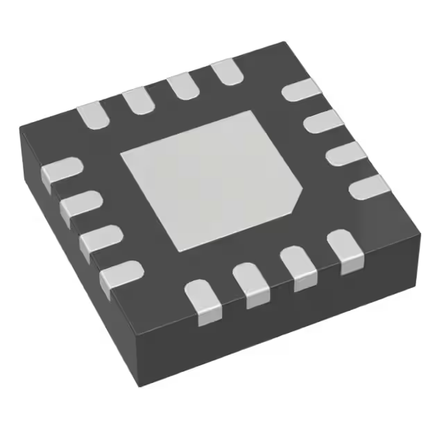
- Part No.:
- TLK6201EARGTT
- Manufacturer:
- Texas Instruments
- Category:
- Specialized
- Package:
- 16-VFQFN Exposed Pad
- Datasheet:
-
 TLK6201EARGTT.pdf
- Description:
- IC INTERFACE SPECIALIZED 16QFN
- Quantity:
- Payment:

- Shipping:

Inventory:3,091
Please send an inquiry. Send us your inquiry, and we will respond immediately.
Product details
Overview
TLK6201EARGTT from Texas Instruments is a 6.25-Gbps multirate cable and PCB equalizer with fixed high-frequency boost (13 dB at 3.125 GHz), four-level output de-emphasis (0/–4/–8/–12 dB), and CML I/Os. It compensates up to 13-dB receive-side loss and 12-dB transmit-side loss on FR4 backplanes or 24-AWG cables, enabling reliable 6.25-Gbps operation over 60 inches of FR4 or 63 feet of cable in PCIe, SAS, and InfiniBand links.
For engineers reviewing the TLK6201EARGTT datasheet, TLK6201EARGTT pinout, TLK6201EARGTT application, or TLK6201EARGTT equivalent, this device delivers deterministic jitter under 12 psP-P, input sensitivity down to 40 mVP-P, ultralow power (54 mA typical), integrated LOS detection, and polarity/swing/de-emphasis control - all in a 3-mm × 3-mm QFN package for high-density serial link designs.
Technical Context
The TLK6201EARGTT implements a fixed-gain, high-speed analog data path comprising three cascaded gain stages, an offset cancellation loop (with COC0/COC1 filter terminals), and a CML output buffer with programmable swing (via SWG) and polarity inversion (via POL). Its equalization is non-adaptive: the 13-dB high-frequency boost is fixed at 3.125 GHz, and de-emphasis levels are selected digitally via DE0/DE1 CMOS inputs.
Loss-of-signal detection uses a fixed threshold comparator on the second gain stage output, asserting LOS when low-frequency input amplitude falls below 40–75 mVP-P; the LOS output can directly drive DIS to implement hardware squelch. The device operates from a single 3.3-V ±10% supply and is characterized from –40°C to 85°C.
Key Specifications
| Parameter | Value and Actual Design Meaning |
|---|---|
| Max Data Rate | 6.25 Gbps - supports PCI Express Gen2, SAS-2, and CEI-6G serial protocols without retiming. |
| Input Sensitivity | 40 mVP-P min - enables recovery of severely attenuated signals after long FR4 traces or cables. |
| High-Frequency Boost | 13 dB at 3.125 GHz - compensates frequency-dependent loss in interconnects up to 13 dB at Nyquist. |
| Output De-Emphasis | 0 / –4 / –8 / –12 dB - selectable via DE0/DE1 to match channel loss profiles and reduce ISI. |
| Differential Output Swing | 600–1500 mVP-P - adjustable 50% increase via SWG pin; compatible with 50-Ω CML receivers. |
| Supply Current | 54 mA typical at 3.3 V - enables low-power high-speed equalization in thermally constrained systems. |
| Deterministic Jitter | 12 psP-P max - ensures clean eye opening at 6.25 Gbps over 36-inch FR4 striplines. |
Pinout & Package
TLK6201EARGTT is housed in a 3-mm × 3-mm, 16-pin VQFN (RGT) package with 0.5-mm pitch and exposed thermal pad (EP). The package requires soldering the EP to PCB ground for thermal and mechanical stability.
| Pin/Terminal | Circuit Role | Design Meaning |
|---|---|---|
| DIN+, DIN– | Differential analog input | Accepts 100-Ω terminated CML/LVDS signals; supports input swings from 40 to 2000 mVP-P. |
| DOUT+, DOUT– | Differential CML output | 50-Ω back-terminated to VCC; swing configurable via SWG; polarity invertible via POL. |
| DE0, DE1 | CMOS de-emphasis select | Set 4 discrete de-emphasis levels (0/–4/–8/–12 dB); internally pulled up. |
| DIS | CMOS output disable | Asserting high disables CML outputs (high-Z state); internally pulled down. |
| LOS | CMOS loss-of-signal indicator | Open-drain output; asserts high when input amplitude drops below 40–75 mVP-P. |
| COC0, COC1 | Analog offset cancellation filter | Connect external capacitor between pins to extend low-frequency cutoff below 3.5 kHz. |
| VCC (pins 9, 12) | Power supply | Single 3.3-V ±10% supply; decoupling required near each VCC pin. |
| GND (pins 1, 4, EP) | Ground reference | All grounds must be low-inductance; EP must be soldered to solid ground plane. |
Key Features
| Feature | Design Value |
|---|---|
| Fixed 13-dB receive equalization at 3.125 GHz | Compensates worst-case FR4 trace loss without adaptive overhead or latency. |
| Four-level programmable transmit de-emphasis | Matches channel insertion loss slope to suppress inter-symbol interference in long cables/backplanes. |
| Integrated loss-of-signal detection with squelch support | Enables automatic output muting when signal disappears - no external logic needed. |
| On-chip offset cancellation with external filter option | Maintains DC balance and low-jitter output across wide input swing range (40–2000 mVP-P). |
| 50% programmable output swing boost | Increases signal margin into lossy receivers or long stubs via simple SWG pin control. |
Applications
| PCI Express Gen2 Backplane Interconnect | SAS-2 Daughtercard Link |
|---|---|
Use Scenario: 6.25-Gbps differential signaling across a 24-layer FR4 backplane with 36-inch stripline routing and 13-dB loss at 3.125 GHz. IC Role / Device Role / Timing Role: Receive-side equalizer restoring signal integrity before CDR in host controller; transmit-side de-emphasis pre-compensating for channel loss. Use Value: Enables full Gen2 compliance without redesigning stackup or adding repeaters - maintains BER <10−12 with <12 psP-P DJ. |
Use Scenario: High-reliability 6.25-Gbps connection between SAS initiator and expander on separate daughtercards linked by flexible ribbon cable. IC Role / Device Role / Timing Role: Bidirectional equalizer placed at both ends of the cable interface to compensate asymmetric loss and maintain eye height/width. Use Value: Supports 63-ft 24-AWG cable reach while meeting SAS-2 jitter and amplitude specs - eliminates need for active cables or retimers. |
| InfiniBand QDR Channel Extension | Fibre Channel 4G/8G Interoperability |
Use Scenario: Extending QDR InfiniBand links beyond standard 15-meter copper limit using custom 24-AWG twinax cable with >10-dB loss at 4 GHz. IC Role / Device Role / Timing Role: Transmit de-emphasis and receive equalization block in switch port PHY, configured for –8 dB de-emphasis and 13 dB boost. Use Value: Achieves stable 40-Gbps aggregate bandwidth over extended distances with deterministic jitter under 10 psP-P. |
Use Scenario: Interfacing legacy 4G FC (4.25 Gbps) and newer 8G FC (8.5 Gbps) equipment via shared copper infrastructure with variable loss profiles. IC Role / Device Role / Timing Role: Multirate equalizer supporting both rates; configured per-link via DE0/DE1 and SWG to optimize for each protocol's loss budget. Use Value: Provides seamless migration path - same hardware supports 4G/8G without firmware or layout changes. |
Equivalent & Alternatives
The following parts are listed as comparable options for similar high-speed equalizer applications.
| Alternative Part | Technical Difference | Application Difference | Selection Advice |
|---|---|---|---|
| MAX3801ETM+ | 3.2-Gbps max rate; 10-dB boost; no integrated LOS or de-emphasis; requires dual supplies. | Limited to ≤3.2 Gbps protocols (e.g., Gigabit Ethernet); lacks squelch and programmable de-emphasis. | Select only for cost-sensitive ≤3.2 Gbps designs where feature set reduction is acceptable. |
| DS100BR210SQ/NOPB | 10.3-Gbps max rate; adaptive CTLE + DFE; 1.8-V core + 3.3-V I/O; higher power (120 mA). | Supports PCIe Gen3/Gen4 and 10G-KR; adds digital adaptation but increases complexity and BOM count. | Choose for next-gen protocols requiring >6.25 Gbps or adaptive equalization; not drop-in compatible. |
Compared with MAX3801ETM+ and DS100BR210SQ/NOPB, TLK6201EARGTT uniquely balances 6.25-Gbps performance, fixed low-latency equalization, integrated LOS/squelch, and ultralow power in a compact QFN - making it optimal for Gen2 serial links where simplicity, predictability, and thermal efficiency are critical.
Availability
TLK6201EARGTT is available at Aetrix Electronics and suitable for PCIe Gen2 backplanes, SAS-2 storage interconnects, and InfiniBand QDR channel extensions requiring stable component supply, long-term lifecycle support, and RoHS-compliant packaging.
Supply support for TLK6201EARGTT includes scheduled delivery planning, volume procurement assistance, BOM continuity management, traceable sourcing, and lifecycle availability coordination for OEM customers, industrial embedded developers, connected-device designers, and electronics production programs.
Manufacturer
Texas Instruments is a global semiconductor leader specializing in analog, embedded processing, and high-speed interface solutions, with decades of expertise in signal integrity and serial link ICs.
The TLK6201EARGTT belongs to TI's high-speed equalizer product line, designed specifically for multirate compensation of lossy copper interconnects in enterprise storage, communications, and computing infrastructure.
FAQ
What is the maximum supported data rate for TLK6201EARGTT?
The TLK6201EARGTT supports a maximum data rate of 6.25 Gbps, validated with K28.5 patterns and BER <10−12 over standard FR4 striplines and 24-AWG cables. This rate aligns with PCI Express Gen2, SAS-2, and InfiniBand QDR specifications. Operation at lower rates (e.g., 2.125 Gbps or 4.25 Gbps) is fully supported with maintained jitter and sensitivity performance.
Does TLK6201EARGTT require external configuration or firmware?
No, TLK6201EARGTT is a fully analog, pin-strapped equalizer with no firmware, registers, or serial interface. Configuration is achieved solely through CMOS logic levels applied to DE0, DE1, POL, SWG, and DIS pins. All equalization, de-emphasis, and squelch functions operate autonomously after power-up and pin state stabilization.
How does the loss-of-signal (LOS) detection work in TLK6201EARGTT?
The TLK6201EARGTT monitors low-frequency components of the signal at the second gain stage output and compares them to a fixed internal threshold (40–75 mVP-P). When input amplitude falls below this level, LOS asserts high. Connecting LOS to DIS creates a self-contained squelch function that disables outputs automatically - eliminating chattering during signal loss events without external logic.
Can TLK6201EARGTT be used with AC-coupled interfaces?
Yes, TLK6201EARGTT is designed for AC-coupled operation. The input and output CML interfaces use on-chip 50-Ω terminations to VCC, and only require external AC-coupling capacitors (C1–C4 in Figure 4). The internal offset cancellation loop handles DC drift, and optional external COC0/COC1 capacitors extend low-frequency response if needed for very low data-rate components.
What thermal considerations apply to TLK6201EARGTT's exposed pad (EP)?
The exposed thermal pad (EP, pin 16) of TLK6201EARGTT must be soldered to a solid PCB ground plane to ensure proper thermal dissipation and mechanical reliability. TI recommends ≥85% solder coverage under the pad and use of thermal vias to inner ground layers. Failure to connect EP results in elevated junction temperature, potentially exceeding the 125°C absolute maximum and degrading jitter or longevity.
TLK6201EARGTT Specifications
- Product attributes
- Attribute value
- Manufacturer:
- Texas Instruments
- Series:
- -
- Package/Case:
- 16-VFQFN Exposed Pad
- Packaging:
- Tape & Reel (TR)
- Product Status:
- Obsolete
- Applications:
- Digital High-Speed Link
- Interface:
- Differential
- Voltage - Supply:
- 3V ~ 3.6V
- Supplier Device Package:
- 16-VQFN (3x3)
- Grade:
- -
- Qualification:
- -
- Mounting Type:
- Surface Mount
TLK6201EARGTT FAQ
1.How can I place an order for TLK6201EARGTT through Aetrix?
Please submit a Request for Quotation (RFQ) for TLK6201EARGTT on Aetrix. Our sales agent will provide a competitive quotation and guide you through the order confirmation once you accept the terms.
2.Are the price and stock information for TLK6201EARGTT reliable?
The price and inventory of TLK6201EARGTT are updated periodically and may fluctuate due to market conditions. Stock and pricing data are typically refreshed every 24 hours. Quotation validity for TLK6201EARGTT is usually 5 days.
3.What payment methods are accepted for TLK6201EARGTT?
We accept Wire Transfer, PayPal, Credit Card, Western Union, MoneyGram, and Escrow for TLK6201EARGTT transactions.
Note: Certain payment methods may incur a processing fee.
4.How is shipping managed for TLK6201EARGTT?
TLK6201EARGTT orders can be shipped via leading logistics carriers, including DHL, UPS, FedEx, TNT, or Registered Mail.
Once your TLK6201EARGTT order is processed, you will receive an email with the shipment details and tracking number.
Note: Tracking information may take up to 24 hours to appear. Express delivery typically takes 3–5 business days.
5.How can I obtain technical support or documentation for TLK6201EARGTT?
For technical support, including TLK6201EARGTT datasheets, pinout diagrams, or application guidance, please contact our engineering support team. They can provide detailed documentation and assistance for your TLK6201EARGTT requirements.
6.How does Aetrix verify that TLK6201EARGTT is sourced from the original manufacturer or authorized distributors?
All TLK6201EARGTT products on Aetrix are procured from qualified distributors and authorized channels. Our dedicated quality assurance team conducts strict verification, including traceability checks and, if necessary, third-party testing. This ensures that TLK6201EARGTT meets industry standards.
7.What is the process for return or replacement of TLK6201EARGTT?
All TLK6201EARGTT units undergo pre-shipment inspection (PSI). If there is an issue with TLK6201EARGTT, returns or replacements are accepted under the following conditions:
1.Quantity discrepancies, incorrect items, or visible external defects (such as breakage or corrosion), acknowledged by Aetrix.
2.The issue is reported within 90 days of delivery.
3.The TLK6201EARGTT part is unused and in its original packaging.
Return procedure for TLK6201EARGTT:
1.Submit a request within 90 days.
2.Obtain a Return Material Authorization (RMA) from Aetrix.
TLK6201EARGTT Tags

-
NVT4857UKAZ
NXP Semiconductors

-
TCA8418RTWR
Texas Instruments

-
PCA9546APWR
Texas Instruments

-
MD0100N8-G
Microchip Technology

-
PCA9548APW,118
NXP Semiconductors

-
PCA9540BDP,118
NXP Semiconductors

-
PCA9548APWR
Texas Instruments

-
PCA9546APW,118
NXP Semiconductors

-
PTN3360DBS,518
NXP Semiconductors

-
PCA9546ABS,118
NXP Semiconductors

-
PCA9518PWR
Texas Instruments

-
PCA9545APW,118
NXP Semiconductors
Tech Hub

A practical engineering guide to 3.3V and 5V logic compatibility, input thresholds, resistor dividers, translator ICs, MOSFET level shifting, I2C pull-ups, timing limits and power-sequencing risks.

The 74HC595 uses push-pull logic outputs, while the TPIC6B595 uses 50 V open-drain DMOS sinks for higher-power loads. This guide compares timing, current limits, 3.3 V interfacing, load wiring, thermal…

The 74HC595 converts serial data into eight stable parallel outputs. This guide covers pin functions, shift and storage timing, OE and MR behavior, drive-current limits, cascading, voltage compatibilit…

A technical comparison of level-sensitive latches and edge-triggered flip-flops, covering timing windows, setup and hold limits, master–slave operation, time borrowing, race-through, HDL inference and…

A D latch stores one bit while Enable controls when data can pass. This reference covers gate-level operation, truth tables, transparency, setup and hold timing, LE versus OE, common ICs and practical …

An SR latch stores one bit through cross-coupled feedback. This engineering reference covers NOR and NAND implementations, truth tables, forbidden-state recovery, gated operation, switch debouncing, fa…

Latch circuits retain one bit through feedback. This technical reference covers SR and D latches, truth tables, transparency, timing limits, latch-versus-flip-flop behavior, applications and common log…

An engineering guide to LED driver operation, constant-current and constant-voltage outputs, linear and switching topologies, dimming, IC selection, calculations, replacement compatibility, and fault c…

Operational amplifier guide covering op amp basics, feedback, ideal vs real op amps, common configurations, buffer circuits, offset, bias current, gain-bandwidth, slew rate, rail-to-rail limits and sel…

Jumper cables guide covering safe connection order, red and black clamp placement, final ground connection, cable gauge, length, clamp quality, copper vs CCA cables, jump starter comparison and battery…


