
 My Inquiry
 My Account


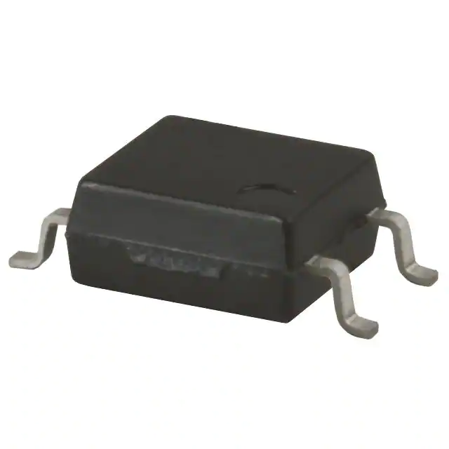
Toshiba Semiconductor and Storage TLP171D(TP,F

- Part No.:
- TLP171D(TP,F
- Manufacturer:
- Toshiba Semiconductor and Storage
- Category:
- Solid State Relays (SSR)
- Package:
- 4-SOP (0.173", 4.40mm)
- Datasheet:
-
 TLP171D(TP,F.pdf
- Description:
- SSR RELAY SPST-NO 200MA 0-200V
- Quantity:
- Payment:

- Shipping:

Inventory:2,199
Please send an inquiry. Send us your inquiry, and we will respond immediately.
Product details
Overview
TLP171D(TP,F) from Toshiba Electronic Devices & Storage Corporation is a normally-open photorelay IC comprising an infrared LED optically coupled to a photo-MOSFET output stage. It delivers 200 V OFF-state voltage, 200 mA ON-state current, and 8 Ω max ON-resistance in a compact SOP-4 package with 2.54 mm pitch - enabling solid-state replacement of mechanical relays in low-power signal switching applications such as PBX line interface cards and security system I/O modules.
For engineers reviewing the TLP171D(TP,F) datasheet, TLP171D(TP,F) pinout, TLP171D(TP,F) application, or TLP171D(TP,F) equivalent, key selection criteria include verified trigger LED current (≤0.2 mA for t >1 s), isolation voltage (1500 Vrms), and dual-drain output configuration suitable for single-pole, single-throw (1-Form-A) AC/DC load control without external snubbers.
Technical Context
The TLP171D(TP,F) implements optical isolation between input and output stages using GaAs infrared LED excitation of a silicon photo-MOSFET. Its internal structure treats Pins 1–2 as a single anode–cathode pair and Pins 3–4 as paralleled drain terminals - forming a two-terminal output device with inherent bidirectional blocking capability up to 200 V.
It operates with low drive power: only 0.2 mA LED forward current sustains conduction at ambient temperatures above 1 s, while maintaining <1 nA OFF-state leakage at rated VOFF. Switching times are specified at 1–10 ms range under 20 V supply and 200 Ω load, supporting moderate-speed digital I/O and analog signal routing where galvanic separation is mandatory.
Key Specifications
| Parameter | Value and Actual Design Meaning |
|---|---|
| OFF-state voltage | 200 V min - supports direct switching of 120 VAC line-powered circuits without external voltage clamping |
| ON-state current | 200 mA max - drives small solenoids, LEDs, or logic-level inputs without external buffering |
| ON-resistance | 8 Ω max - limits power dissipation to ≤320 mW at full load, enabling operation without heatsinking |
| Trigger LED current | 0.2 mA max (t >1 s) - reduces MCU GPIO current burden and enables battery-powered remote sensing |
| Isolation voltage | 1500 Vrms min - meets UL 1577 and CSA Component Acceptance for reinforced insulation in Class II systems |
| Package | SOP-4 (11-5H1S), 2.54 mm pitch, 2.1 mm height - compatible with standard 0.1" header footprints and automated SMT assembly |
Pinout & Package
Package: SOP-4 (Toshiba designation 11-5H1S), surface-mount, 2.54 mm lead pitch, 2.1 mm profile, 0.1 g typical weight.
| Pin/Terminal | Circuit Role | Design Meaning |
|---|---|---|
| 1 | Anode | LED anode input; must be driven with current-limited source (e.g., series resistor from 3.3/5 V) |
| 2 | Cathode | LED cathode return; connects to ground or low-side switch |
| 3 | Drain | Output drain terminal; internally shorted to Pin 4 for parallel current handling |
| 4 | Drain | Output drain terminal; shares same node as Pin 3 per datasheet Note 1 |
Key Features
| Feature | Design Value |
|---|---|
| Normally-open (1-Form-A) | Zero static power draw in OFF state; eliminates standby current in always-on control systems |
| Dual-drain output configuration | Reduces effective RON and thermal stress by distributing 200 mA across two bonded die terminals |
| Low trigger LED current | Enables direct drive from ultra-low-power microcontrollers (e.g., ARM Cortex-M0+ GPIOs) without buffer transistors |
| UL/cUL recognized isolation | Validated safety compliance eliminates need for additional certification testing in end-equipment medical or industrial designs |
Applications
| Security System I/O Modules | Modem/Fax PC Cards |
|---|---|
Use Scenario: Isolated status reporting and alarm triggering in door/window sensor interfaces. IC Role / Device Role / Timing Role: Solid-state relay replacing electromechanical units for dry-contact simulation and tamper detection. Use Value: Eliminates contact bounce, extends service life beyond 107 cycles, and reduces PCB space by 40% vs. equivalent mechanical relays. | Use Scenario: Line-level signal switching between analog front-end and controller in legacy dial-up modems. IC Role / Device Role / Timing Role: Bidirectional AC-coupled signal path isolator with 200 V blocking capability. Use Value: Prevents ground loop noise and protects host logic from line surges without requiring transformer-based isolation. |
| Private Branch Exchanges (PBXs) | Measuring Instruments |
Use Scenario: Ring detect and line seizure control in analog telephone interface cards. IC Role / Device Role / Timing Role: High-voltage, low-leakage switch for supervisory signaling on POTS lines. Use Value: Maintains <1 nA OFF-state leakage at 200 V, ensuring reliable ring detection without false triggers. | Use Scenario: Multiplexer channel selection in portable multimeters and data loggers. IC Role / Device Role / Timing Role: Low-RON, low-charge-injection analog switch for precision DC voltage routing. Use Value: 8 Ω RON and <90 pF output capacitance minimize measurement error and settling time in sub-100 µV ranges. |
Equivalent & Alternatives
The following parts are listed as comparable options for similar photorelay applications.
| Alternative Part | Technical Difference | Application Difference | Selection Advice |
|---|---|---|---|
| PVG612A | Higher 400 V VOFF, but 12 Ω RON and 0.5 mA IFT; SO-6 package | Better suited for 240 VAC mains monitoring; less optimal for low-voltage precision analog switching | Select when higher blocking voltage outweighs ON-resistance penalty and SO-6 footprint is acceptable |
| PS8501-AX | Same SOP-4, 200 V VOFF, but 10 Ω RON and 0.3 mA IFT; lower isolation (5000 Vp) | Compatible pinout but higher drive requirement; reduced creepage for space-constrained designs | Choose if existing layout uses PS8501 footprint and 0.3 mA LED drive is available |
Compared with PVG612A and PS8501-AX, the TLP171D(TP,F) offers the lowest trigger current (0.2 mA) and tightest RON (8 Ω) in SOP-4, making it optimal for battery-powered or low-noise analog signal routing where minimal drive power and voltage drop are critical.
Availability
TLP171D(TP,F) is available at Aetrix Electronics and suitable for security system I/O modules, modem/fax PC cards, and measuring instruments requiring stable component supply, long-term lifecycle support, and RoHS-compliant sourcing.
Supply support for TLP171D(TP,F) includes scheduled delivery planning, volume procurement assistance, BOM continuity management, traceable sourcing, and lifecycle availability coordination for OEM customers, industrial embedded developers, connected-device designers, and electronics production programs.
Manufacturer
Toshiba Electronic Devices & Storage Corporation designs and manufactures discrete semiconductors, power devices, and optoelectronics for industrial, consumer, and communications markets.
The TLP171D(TP,F) belongs to Toshiba's photorelay product line, engineered specifically for mechanical relay replacement in space-constrained, low-power, and high-reliability signal switching applications.
FAQ
What is the maximum continuous ON-state current rating for the TLP171D(TP,F)?
The TLP171D(TP,F) supports a maximum continuous ON-state current of 200 mA at Ta ≤ 25 °C. Derating applies linearly at −2.0 mA/°C above 25 °C, limiting usable current to approximately 160 mA at 45 °C ambient. This rating assumes proper PCB copper area for thermal dissipation and accounts for the device's 8 Ω max RON to ensure junction temperature remains within 125 °C limit. The TLP171D(TP,F) is not rated for pulsed currents exceeding 600 mA.
Does the TLP171D(TP,F) support AC load switching?
Yes, the TLP171D(TP,F) supports bidirectional AC load switching due to its MOSFET-based output structure and 200 V minimum OFF-state voltage rating. Its symmetrical drain terminals (Pins 3 and 4) allow connection across either polarity of an AC waveform, provided peak voltage remains below 200 V. The TLP171D(TP,F) exhibits <1 nA OFF-state leakage at rated VOFF, ensuring reliable zero-crossing detection and minimal power loss during AC idle periods.
What is the recommended LED forward current for reliable turn-on of the TLP171D(TP,F)?
Toshiba specifies a maximum trigger LED current of 0.2 mA for sustained conduction (t >1 s) and 0.1 mA for short pulses (t ≤1 s). A design target of 0.5 mA provides robust margin against aging and temperature drift while staying well within the 30 mA absolute maximum rating. The TLP171D(TP,F)'s low IFT enables direct drive from most microcontroller GPIOs using a simple 10 kΩ series resistor from 5 V or 6.8 kΩ from 3.3 V.
How is isolation performance validated for the TLP171D(TP,F)?
The TLP171D(TP,F) is UL-recognized per UL 1577 (File No. E67349) and cUL-recognized per CSA Component Acceptance Service (File No. E67349), with minimum isolation voltage of 1500 Vrms tested for 60 seconds. Its isolation resistance exceeds 5 × 10¹⁰ Ω and input-to-output capacitance is limited to 0.8 pF typical - verified via factory production testing per Toshiba's quality protocol. These values are guaranteed across the full operating temperature range (−40 to +85 °C) and apply to the TLP171D(TP,F) in its final packaged form.
Can the TLP171D(TP,F) replace mechanical relays in PBX line interface circuits?
Yes, the TLP171D(TP,F) is explicitly qualified for Private Branch Exchange (PBX) applications per Toshiba's datasheet. Its 200 V OFF-state voltage safely handles POTS line ringing voltages (typically 90 V RMS, ~127 V peak), while its <1 nA OFF-state leakage prevents false ring detection. With 3.5 ms typical turn-on time and no contact wear, the TLP171D(TP,F) delivers >108 operations versus ~105 for equivalent mechanical relays - making it ideal for high-cycle PBX line seizure and status reporting functions.
TLP171D(TP,F Specifications
- Product attributes
- Attribute value
- Manufacturer:
- Toshiba Semiconductor and Storage
- Series:
- TLP171D
- Packaging:
- Tape & Reel (TR)
- Product Status:
- Active
- Mounting Type:
- Surface Mount
- Circuit:
- SPST-NO (1 Form A)
- Output Type:
- AC, DC
- Voltage - Input:
- 1.27VDC
- Voltage - Load:
- 0 V ~ 200 V
- Load Current:
- 200 mA
- On-State Resistance (Max):
- 8 Ohms
- Termination Style:
- Gull Wing
- Operating Temperature:
- -40°C ~ 85°C
- Supplier Device Package:
- 4-SOP
- Approval Agency:
- cUL, UL, VDE
- Grade:
- -
- Qualification:
- -
TLP171D(TP,F FAQ
1.How can I place an order for TLP171D(TP,F through Aetrix?
Please submit a Request for Quotation (RFQ) for TLP171D(TP,F on Aetrix. Our sales agent will provide a competitive quotation and guide you through the order confirmation once you accept the terms.
2.Are the price and stock information for TLP171D(TP,F reliable?
The price and inventory of TLP171D(TP,F are updated periodically and may fluctuate due to market conditions. Stock and pricing data are typically refreshed every 24 hours. Quotation validity for TLP171D(TP,F is usually 5 days.
3.What payment methods are accepted for TLP171D(TP,F?
We accept Wire Transfer, PayPal, Credit Card, Western Union, MoneyGram, and Escrow for TLP171D(TP,F transactions.
Note: Certain payment methods may incur a processing fee.
4.How is shipping managed for TLP171D(TP,F?
TLP171D(TP,F orders can be shipped via leading logistics carriers, including DHL, UPS, FedEx, TNT, or Registered Mail.
Once your TLP171D(TP,F order is processed, you will receive an email with the shipment details and tracking number.
Note: Tracking information may take up to 24 hours to appear. Express delivery typically takes 3–5 business days.
5.How can I obtain technical support or documentation for TLP171D(TP,F?
For technical support, including TLP171D(TP,F datasheets, pinout diagrams, or application guidance, please contact our engineering support team. They can provide detailed documentation and assistance for your TLP171D(TP,F requirements.
6.How does Aetrix verify that TLP171D(TP,F is sourced from the original manufacturer or authorized distributors?
All TLP171D(TP,F products on Aetrix are procured from qualified distributors and authorized channels. Our dedicated quality assurance team conducts strict verification, including traceability checks and, if necessary, third-party testing. This ensures that TLP171D(TP,F meets industry standards.
7.What is the process for return or replacement of TLP171D(TP,F?
All TLP171D(TP,F units undergo pre-shipment inspection (PSI). If there is an issue with TLP171D(TP,F, returns or replacements are accepted under the following conditions:
1.Quantity discrepancies, incorrect items, or visible external defects (such as breakage or corrosion), acknowledged by Aetrix.
2.The issue is reported within 90 days of delivery.
3.The TLP171D(TP,F part is unused and in its original packaging.
Return procedure for TLP171D(TP,F:
1.Submit a request within 90 days.
2.Obtain a Return Material Authorization (RMA) from Aetrix.
TLP171D(TP,F Tags
.jpg)
-
G3VM-21UR11(TR05)
Omron Electronics Inc-EMC Div
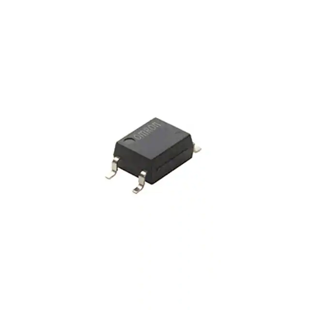
-
G3VM-61VY3(TR05)
Omron Electronics Inc-EMC Div
-
CPC1017NTR
Littelfuse Inc.
-
CPC1017N
Littelfuse Inc.
-
CPC1006N
Littelfuse Inc.
-
VO1400AEFTR
Vishay Semiconductor Opto Division
-
CPC1006NTR
Littelfuse Inc.
-
TLP175A(TPL,E
Toshiba Semiconductor and Storage
-
CPC1002NTR
Littelfuse Inc.
-
AQY280S
Panasonic Electric Works
-
CPC1117NTR
Littelfuse Inc.
-
CPC1106NTR
Littelfuse Inc.
Tech Hub

Counterfeit components can hide behind convincing markings and passing basic function tests. This engineering reference covers source traceability, external inspection, X-ray, XRF, electrical testing, …

A practical engineering and sourcing framework covering lifecycle verification, lifetime-buy calculations, replacement qualification, supplier checks and counterfeit-risk controls.

TTL and CMOS logic families differ in thresholds, loading, output drive, power and timing. This engineering guide compares 74HC and 74HCT, calculates noise margins and checks 3.3 V/5 V compatibility.

A practical engineering guide to 3.3V and 5V logic compatibility, input thresholds, resistor dividers, translator ICs, MOSFET level shifting, I2C pull-ups, timing limits and power-sequencing risks.

The 74HC595 uses push-pull logic outputs, while the TPIC6B595 uses 50 V open-drain DMOS sinks for higher-power loads. This guide compares timing, current limits, 3.3 V interfacing, load wiring, thermal…

The 74HC595 converts serial data into eight stable parallel outputs. This guide covers pin functions, shift and storage timing, OE and MR behavior, drive-current limits, cascading, voltage compatibilit…

A technical comparison of level-sensitive latches and edge-triggered flip-flops, covering timing windows, setup and hold limits, master–slave operation, time borrowing, race-through, HDL inference and…

A D latch stores one bit while Enable controls when data can pass. This reference covers gate-level operation, truth tables, transparency, setup and hold timing, LE versus OE, common ICs and practical …

An SR latch stores one bit through cross-coupled feedback. This engineering reference covers NOR and NAND implementations, truth tables, forbidden-state recovery, gated operation, switch debouncing, fa…

Latch circuits retain one bit through feedback. This technical reference covers SR and D latches, truth tables, transparency, timing limits, latch-versus-flip-flop behavior, applications and common log…


