
 My Inquiry
 My Account


Toshiba Semiconductor and Storage TLP2166A(TP,F)
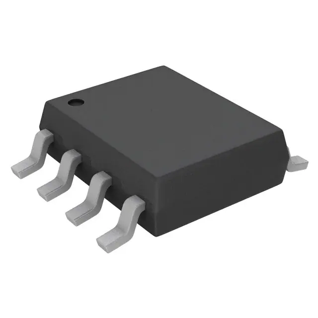
- Part No.:
- TLP2166A(TP,F)
- Manufacturer:
- Toshiba Semiconductor and Storage
- Category:
- Logic Output Optoisolators
- Package:
- 8-SOIC (0.154", 3.90mm Width)
- Datasheet:
-
 TLP2166A(TP,F).pdf
- Description:
- OPTOISO 2.5KV 2CH PUSH PULL 8SO
- Quantity:
- Payment:

- Shipping:

Inventory:4,987
Please send an inquiry. Send us your inquiry, and we will respond immediately.
Product details
Overview
TLP2166A(TP,F) from Toshiba Electronic Devices & Storage Corporation is a dual-channel, high-speed photovoltaic coupler with totem-pole logic outputs, designed for isolated digital signal transmission in 3.3-V systems. It integrates two independent IRED–photodetector pairs in one SO8 package, delivers 15 MBd NRZ data rate, achieves ≤75 ns propagation delay, and sustains operation across –40°C to +100°C - enabling use in plasma display panel (PDP) scan drivers and industrial high-speed serial interfaces.
For engineers reviewing the TLP2166A(TP,F) datasheet, TLP2166A(TP,F) pinout, TLP2166A(TP,F) application, or TLP2166A(TP,F) equivalent, key selection criteria include guaranteed 3.3-V supply compatibility, ±15 kV/μs common-mode transient immunity, dual-channel isolation with independent anode/cathode terminals, and UL/cUL/VDE safety certifications supporting reinforced insulation in safety-critical control loops.
Technical Context
The TLP2166A(TP,F) implements two fully independent optically isolated channels, each combining a GaAs infrared LED with a monolithic high-gain photodetector IC featuring totem-pole output stage. Its logic inversion behavior (LED ON → output LOW) and strict 3.0–3.6 V VCC range are fixed by internal detector biasing and threshold design.
Isolation performance relies on internal shielded die construction and molded SO8 package geometry, delivering 2500 Vrms withstand voltage and <0.8 pF input-to-output capacitance. Common-mode transient immunity is achieved via differential sensing and internal shielding between input and output sections, validated at ±15 kV/μs under defined test conditions.
Key Specifications
| Parameter | Value and Actual Design Meaning |
|---|---|
| Supply Voltage | 3.0–3.6 V - mandates external 3.3-V rail; operation below 3.0 V risks unstable output or elevated ICCH. |
| Max Switching Speed | 15 MBd (NRZ, typ.) - supports high-frequency serial protocols such as RS-422/485 isolators or PDP address drivers. |
| Propagation Delay | ≤75 ns (tpHL/tpLH) - enables sub-100 ns digital edge transmission across isolation barrier for real-time control. |
| Input Threshold Current | IFHL ≤ 3 mA - ensures reliable logic LOW detection with low-drive microcontrollers or FPGA I/Os. |
| Common-Mode Immunity | ±15 kV/μs - suppresses fast transients from motor drives or power converters without output corruption. |
| Isolation Voltage | 2500 Vrms - meets reinforced insulation requirements per UL 1577 and EN 60747-5-5 (with V4 option). |
| Operating Temperature | –40°C to +100°C - qualified for industrial motor control, HVAC, and PDP subsystems without derating. |
Pinout & Package
The TLP2166A(TP,F) is housed in an 8-pin Small Outline (SO8) package per JEDEC MS-012, with 1.27 mm pitch, 5.0 mm body width, and 0.11 g typical mass. A 0.1 μF ceramic bypass capacitor must be placed between pins 8 (VCC) and 5 (GND), with total lead length ≤1 cm.
| Pin/Terminal | Circuit Role | Design Meaning |
|---|---|---|
| 1: ANODE 1 | LED Channel 1 anode | Connects to 3.3-V source via current-limiting resistor; forward voltage ~1.65 V @ 10 mA. |
| 2: CATHODE 1 | LED Channel 1 cathode | Drives logic HIGH when LED is OFF; reverse voltage rating 5 V limits pull-up configuration. |
| 3: CATHODE 2 | LED Channel 2 cathode | Independent second channel input; shares no electrical connection with Channel 1 LED path. |
| 4: ANODE 2 | LED Channel 2 anode | Enables dual isolated inputs without shared current paths - critical for cross-talk–sensitive applications. |
| 5: GND | Detector ground reference | Common return for both output stages; must be tied to system logic ground, not power ground. |
| 6: VO2 (Output 2) | Channel 2 totem-pole output | Active LOW logic output; VOL ≤ 0.6 V @ 1.6 mA sink load; VOH ≥ 2.0 V @ –0.02 mA source. |
| 7: VO1 (Output 1) | Channel 1 totem-pole output | Electrically isolated from VO2; supports independent enable/control signals in multi-axis systems. |
| 8: VCC | Detector supply input | Must be decoupled to Pin 5; supplies both photodetector ICs; max 6 V absolute rating. |
Key Features
| Feature | Design Value |
|---|---|
| Dual-channel integration | Two independent opto-isolators in single SO8 package - reduces PCB area by ~40% vs. discrete solutions. |
| Inverting totem-pole output | No external pull-up required; drives CMOS/TTL loads directly with 10 mA sink/source capability. |
| High CMTI | ±15 kV/μs immunity - maintains signal integrity in noisy environments like servo drive feedback loops. |
| Low inter-channel capacitance | <0.8 pF input-to-output coupling - prevents crosstalk between isolated data and control lines. |
| Industrial temperature range | –40°C to +100°C operation - eliminates need for thermal derating in enclosed industrial enclosures. |
Applications
| Plasma Display Panel (PDP) Scan Driver | Industrial Serial Interface Isolation |
|---|---|
|
Use Scenario: Driving row/column electrode switches in AC plasma display panels where high-voltage switching induces fast transients. IC Role / Device Role / Timing Role: Isolated logic-level translator between low-voltage FPGA controller and high-side gate drivers. Use Value: 75 ns propagation delay ensures precise timing alignment across 1024×768 pixel addressing; ±15 kV/μs CMTI prevents false triggering during sustain pulse transitions. |
Use Scenario: Galvanic isolation of RS-422/485 differential data lines in factory automation PLC backplanes. IC Role / Device Role / Timing Role: Dual-channel unidirectional isolator for TX and RX paths, preserving signal edge fidelity. Use Value: 15 MBd NRZ throughput supports full-duplex 10 Mbps operation; 2500 Vrms isolation meets IEC 61000-4-5 surge immunity requirements. |
| Motor Control Feedback Isolation | Programmable Logic Controller (PLC) Input Module |
|
Use Scenario: Isolating encoder quadrature A/B signals and index pulse from 48 V motor drive circuits. IC Role / Device Role / Timing Role: High-speed digital isolator preserving phase relationship between A/B edges for position tracking. Use Value: ≤45 ns switching dispersion minimizes phase error in 100 kHz encoder streams; dual-channel layout avoids skew between A/B paths. |
Use Scenario: Converting 24 V DC field sensor inputs into clean 3.3 V logic levels for ARM-based PLC CPU modules. IC Role / Device Role / Timing Role: Input channel conditioner providing voltage level shift, noise rejection, and galvanic break. Use Value: IFHL ≤ 3 mA allows direct connection to standard 24 V sink sensors; –40°C to +100°C rating supports operation in unconditioned cabinet environments. |
Equivalent & Alternatives
The following parts are listed as comparable options for similar high-speed digital isolator applications.
| Alternative Part | Technical Difference | Application Difference | Selection Advice |
|---|---|---|---|
| TLP2366(TP,F) | Same SO8 footprint, but rated for 5 V supply (4.5–5.5 V); higher IFHL (5 mA max); identical 75 ns delay and 2500 Vrms isolation. | Requires 5 V logic domain; unsuitable for native 3.3 V systems without level-shifting. | Select when interfacing with 5 V microcontrollers or legacy industrial buses requiring 5 V compatibility. |
| ACPL-M61T-000E | SO5 package, single-channel, 10 MBd speed, 100 ns max delay, 3750 Vrms isolation, operates at 3.3 V with IFHL = 5 mA. | Lacks dual-channel integration; requires two units for same functionality; higher isolation voltage but slower timing. | Choose when board space permits separate channels and higher isolation voltage is prioritized over speed or density. |
Compared with TLP2166A(TP,F), the TLP2366(TP,F) shifts supply compatibility to 5 V at the cost of 3.3 V system readiness, while the ACPL-M61T-000E trades dual-channel integration and 15 MBd speed for higher isolation rating and single-channel simplicity - making TLP2166A(TP,F) optimal for compact, high-speed, 3.3-V–native industrial interfaces.
Availability
TLP2166A(TP,F) is available at Aetrix Electronics and suitable for plasma display panel (PDP) scan drivers, industrial RS-422/485 isolators, and motor encoder feedback circuits requiring stable component supply, long-lifecycle support, and traceable sourcing.
Supply support for TLP2166A(TP,F) includes scheduled delivery planning, volume procurement assistance, BOM continuity management, traceable sourcing, and lifecycle availability coordination for OEM customers, industrial embedded developers, connected-device designers, and electronics production programs.
Manufacturer
Toshiba Electronic Devices & Storage Corporation designs and manufactures high-reliability semiconductor components, with core expertise in optoelectronics, power devices, and storage solutions for industrial and consumer markets.
The TLP2166A(TP,F) belongs to Toshiba's high-speed photocopler family, engineered specifically for noise-immune digital signal isolation in 3.3-V industrial control, display, and automation systems where timing precision and thermal robustness are critical.
FAQ
What is the recommended bypass capacitor for TLP2166A(TP,F) and why is it required?
A 0.1 μF ceramic capacitor must be placed between pin 8 (VCC) and pin 5 (GND) for TLP2166A(TP,F), with total lead length ≤1 cm. This capacitor stabilizes the internal high-gain photodetector amplifier, preventing oscillation and ensuring consistent 75 ns propagation delay and clean logic transitions. Omission causes increased jitter, output instability, or failure to meet 15 MBd NRZ performance - verified in Toshiba's Test Circuit 3 and Application Note AN-102.
Does TLP2166A(TP,F) support 5 V logic inputs or is it strictly 3.3 V only?
TLP2166A(TP,F) is strictly a 3.3 V–optimized device: its recommended operating VCC is 3.0–3.6 V, and operation below 3.0 V risks elevated ICCH and output instability per Toshiba's Recommended Operating Conditions table. While absolute maximum VCC is 6 V, applying 5 V may exceed internal detector bias limits and invalidate the 75 ns timing spec. For 5 V systems, Toshiba recommends TLP2366(TP,F) instead.
How does the TLP2166A(TP,F) achieve ±15 kV/μs common-mode transient immunity?
TLP2166A(TP,F) achieves ±15 kV/μs CMTI through internal shielded die construction, optimized spacing between input and output bond wires, and differential sensing within the photodetector IC. The SO8 package includes internal conductive shielding layers between pins 1–4 (input side) and pins 5–8 (output side), validated per Test Circuit 6 in the datasheet. This architecture rejects fast dV/dt noise without requiring external filtering components.
Can TLP2166A(TP,F) be used in automotive applications?
TLP2166A(TP,F) is not qualified for automotive applications: it lacks AEC-Q100 certification, has no specified PPAP support, and its –40°C to +100°C operating range excludes extended automotive temperature grades (–40°C to +125°C or +150°C). Toshiba explicitly restricts use in transportation systems per its "Restrictions on Product Use" notice. For automotive isolation, consider AEC-Q100–qualified alternatives like Si86xx or ISO77xx series.
What is the meaning of the "(TP,F)" suffix in TLP2166A(TP,F)?
The "(TP,F)" suffix in TLP2166A(TP,F) indicates embossed tape packaging (TP) in a plastic carrier tape with cover tape (F), containing 2500 units per reel. "TP" denotes the tape type per Toshiba's packing specification; "F" specifies the cover tape material (static-dissipative plastic). This differs from tube (T) or bulk (B) packaging and is required for automated SMT placement - confirmed in Toshiba's Packing Specification Document Section 2 and Table 1.
TLP2166A(TP,F) Specifications
- Product attributes
- Attribute value
- Manufacturer:
- Toshiba Semiconductor and Storage
- Series:
- -
- Package/Case:
- 8-SOIC (0.154", 3.90mm Width)
- Packaging:
- Tape & Reel (TR)
- Product Status:
- Active
- Number of Channels:
- 2
- Inputs - Side 1/Side 2:
- 2/0
- Voltage - Isolation:
- 2500Vrms
- Common Mode Transient Immunity (Min):
- 15kV/µs
- Input Type:
- DC
- Output Type:
- Push-Pull, Totem Pole
- Current - Output / Channel:
- 10 mA
- Data Rate:
- 15MBd
- Propagation Delay tpLH / tpHL (Max):
- 75ns, 75ns
- Rise / Fall Time (Typ):
- 5ns, 5ns
- Voltage - Forward (Vf) (Typ):
- 1.65V
- Current - DC Forward (If) (Max):
- 15mA
- Voltage - Supply:
- 3V ~ 3.63V
- Grade:
- -
- Qualification:
- -
- Operating Temperature:
- -40°C ~ 100°C
- Mounting Type:
- Surface Mount
- Supplier Device Package:
- 8-SO
TLP2166A(TP,F) FAQ
1.How can I place an order for TLP2166A(TP,F) through Aetrix?
Please submit a Request for Quotation (RFQ) for TLP2166A(TP,F) on Aetrix. Our sales agent will provide a competitive quotation and guide you through the order confirmation once you accept the terms.
2.Are the price and stock information for TLP2166A(TP,F) reliable?
The price and inventory of TLP2166A(TP,F) are updated periodically and may fluctuate due to market conditions. Stock and pricing data are typically refreshed every 24 hours. Quotation validity for TLP2166A(TP,F) is usually 5 days.
3.What payment methods are accepted for TLP2166A(TP,F)?
We accept Wire Transfer, PayPal, Credit Card, Western Union, MoneyGram, and Escrow for TLP2166A(TP,F) transactions.
Note: Certain payment methods may incur a processing fee.
4.How is shipping managed for TLP2166A(TP,F)?
TLP2166A(TP,F) orders can be shipped via leading logistics carriers, including DHL, UPS, FedEx, TNT, or Registered Mail.
Once your TLP2166A(TP,F) order is processed, you will receive an email with the shipment details and tracking number.
Note: Tracking information may take up to 24 hours to appear. Express delivery typically takes 3–5 business days.
5.How can I obtain technical support or documentation for TLP2166A(TP,F)?
For technical support, including TLP2166A(TP,F) datasheets, pinout diagrams, or application guidance, please contact our engineering support team. They can provide detailed documentation and assistance for your TLP2166A(TP,F) requirements.
6.How does Aetrix verify that TLP2166A(TP,F) is sourced from the original manufacturer or authorized distributors?
All TLP2166A(TP,F) products on Aetrix are procured from qualified distributors and authorized channels. Our dedicated quality assurance team conducts strict verification, including traceability checks and, if necessary, third-party testing. This ensures that TLP2166A(TP,F) meets industry standards.
7.What is the process for return or replacement of TLP2166A(TP,F)?
All TLP2166A(TP,F) units undergo pre-shipment inspection (PSI). If there is an issue with TLP2166A(TP,F), returns or replacements are accepted under the following conditions:
1.Quantity discrepancies, incorrect items, or visible external defects (such as breakage or corrosion), acknowledged by Aetrix.
2.The issue is reported within 90 days of delivery.
3.The TLP2166A(TP,F) part is unused and in its original packaging.
Return procedure for TLP2166A(TP,F):
1.Submit a request within 90 days.
2.Obtain a Return Material Authorization (RMA) from Aetrix.
TLP2166A(TP,F) Tags

-
6N137
Lite-On Inc.
-
6N137S
Lite-On Inc.
-
6N137S-TA1
Lite-On Inc.
.JPG)
-
TLP2362(TPR,E
Toshiba Semiconductor and Storage

-
H11L1M
onsemi
-
TLP2355(TPL,E
Toshiba Semiconductor and Storage
-
TLP2361(TPL,E
Toshiba Semiconductor and Storage
-
TLP2358(TPL,E)
Toshiba Semiconductor and Storage
-
H11L1SR2M
onsemi
-
TLP2361(V4-TPL,E
Toshiba Semiconductor and Storage
.JPG)
-
H11L1S(TA)
Everlight Electronics Co Ltd
-
H11L1SM
onsemi
Tech Hub

Counterfeit components can hide behind convincing markings and passing basic function tests. This engineering reference covers source traceability, external inspection, X-ray, XRF, electrical testing, …

A practical engineering and sourcing framework covering lifecycle verification, lifetime-buy calculations, replacement qualification, supplier checks and counterfeit-risk controls.

TTL and CMOS logic families differ in thresholds, loading, output drive, power and timing. This engineering guide compares 74HC and 74HCT, calculates noise margins and checks 3.3 V/5 V compatibility.

A practical engineering guide to 3.3V and 5V logic compatibility, input thresholds, resistor dividers, translator ICs, MOSFET level shifting, I2C pull-ups, timing limits and power-sequencing risks.

The 74HC595 uses push-pull logic outputs, while the TPIC6B595 uses 50 V open-drain DMOS sinks for higher-power loads. This guide compares timing, current limits, 3.3 V interfacing, load wiring, thermal…

The 74HC595 converts serial data into eight stable parallel outputs. This guide covers pin functions, shift and storage timing, OE and MR behavior, drive-current limits, cascading, voltage compatibilit…

A technical comparison of level-sensitive latches and edge-triggered flip-flops, covering timing windows, setup and hold limits, master–slave operation, time borrowing, race-through, HDL inference and…

A D latch stores one bit while Enable controls when data can pass. This reference covers gate-level operation, truth tables, transparency, setup and hold timing, LE versus OE, common ICs and practical …

An SR latch stores one bit through cross-coupled feedback. This engineering reference covers NOR and NAND implementations, truth tables, forbidden-state recovery, gated operation, switch debouncing, fa…

Latch circuits retain one bit through feedback. This technical reference covers SR and D latches, truth tables, transparency, timing limits, latch-versus-flip-flop behavior, applications and common log…


