
 My Inquiry
 My Account


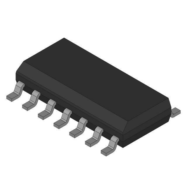
Texas Instruments TLV5590ED
- Part No.:
- TLV5590ED
- Manufacturer:
- Texas Instruments
- Category:
- Analog to Digital Converters (ADC)
- Package:
- -
- Datasheet:
-
 TLV5590ED.pdf
- Description:
- ADC, PROPRIETARY METHOD, 2-BIT
- Quantity:
- Payment:

- Shipping:

Inventory:3,044
Please send an inquiry. Send us your inquiry, and we will respond immediately.
Product details
Overview
TLV5590ED from Texas Instruments is a 2-bit analog-to-digital converter optimized for FLEX protocol pagers, integrating dual-bandwidth (1 kHz/2 kHz ±5% −3 dB) 3rd-order Butterworth filtering, peak/valley detection with auto-adjusting 8-bit DACs, and four selectable acquisition modes - all operating from a single 2.7-V to 3.3-V supply. It directly interfaces with the TLV5591BVF FLEX decoder in numeric/alphanumeric pager baseband signal conditioning.
For engineers reviewing the TLV5590ED datasheet, TLV5590ED pinout, TLV5590ED application, or TLV5590ED equivalent, key selection considerations include its dual-bandwidth filter selectability via BW pin, real-time 2-bit ADC output on EXTS0/EXTS1, TRACKINH-controlled peak/valley tracking enable, and standby mode drawing only 1 µA - critical for battery-powered one-way/two-way pager designs.
Technical Context
The TLV5590ED implements a mixed-signal architecture where a switched-capacitor 3rd-order Butterworth filter precedes a 2-bit ADC whose reference levels (Vref+/Vref−) are dynamically set by two independent 8-bit DACs driven by up/down counters. Filter cutoff is digitally selected between 1 kHz and 2 kHz via the BW input, with nominal gain of 12 dB.
Its digital control logic latches all inputs (CON1, CON2, BW, TRACKINH, TEST) on the falling edge of a 38.4-kHz TTL-level CLK, enabling four operational modes: fast acquisition (attack rate 1.6–2.0 V/s), slow acquisition (0.8–1.0 V/s), hold (DAC outputs frozen), and standby (1 µA quiescent current). Peak/valley tracking is gated by TRACKINH, and decay timing is controlled by dedicated counters reset to 1 or 40 depending on mode.
Key Specifications
| Parameter | Value and Actual Design Meaning |
|---|---|
| ADC Resolution | 2-bit with three internal comparators defining four output levels per FLEX 4-level baseband signal. |
| Filter Bandwidth | Selectable 1 kHz ±5% or 2 kHz ±5% −3 dB cutoff; enables optimal noise rejection for FLEX symbol rates. |
| Supply Voltage | 2.7 V to 3.3 V single supply; supports low-voltage battery operation without level-shifting circuitry. |
| Standby Current | 1 µA at DVDD = 2.7–3.3 V; extends pager battery life during idle periods. |
| CLK Frequency | 38.4 kHz nominal; directly determines filter timing, attack/decay rates, and ADC sampling synchronization. |
| Operating Temp | −25°C to +85°C; qualified for commercial pager environments including handheld thermal cycling. |
| Digital Outputs | EXTS0 (LSB) and EXTS1 (MSB); TTL-compatible, 100 µA drive strength, VOH ≥ DVDD − 0.5 V. |
Pinout & Package
D-package (SOIC-14) surface-mount package with 14-pin dual in-line configuration, 1.27 mm pitch, body width 3.9 mm, and JEDEC MS-012AC compliance.
| Pin/Terminal | Circuit Role | Design Meaning |
|---|---|---|
| DVDD | Digital supply input | Provides power to digital logic, clock interface, and output drivers; must be decoupled near pin. |
| AVDD | Analog supply input | Supplies analog signal path, filters, and DACs; separate from DVDD to minimize digital noise coupling. |
| SIG | Analog signal input | Differential input referenced to DC OFFSET; requires external antialiasing RC filter before this pin. |
| DC OFFSET | Analog dc bias input | Sets quiescent operating point for SIG; enables full-scale utilization of 2-bit ADC without saturation. |
| MID | Analog midpoint output | Buffered AVDD/2 reference (1.42–1.58 V at 3 V); used for biasing external circuitry or as test point. |
| GND | Ground return | Common return for analog and digital currents; layout requires star grounding to avoid crosstalk. |
| BW | Digital bandwidth select | High = 2 kHz filter; Low = 1 kHz filter; sets cutoff before ADC to match FLEX symbol timing. |
| CLK | System clock input | 38.4 kHz TTL-level clock; falling-edge sensitive in normal modes; defines all timing intervals. |
| TEST | Test mode enable | High = enter test mode (0–3); must be grounded in normal operation to prevent unintended behavior. |
| TRACKINH | Tracking inhibit | Low = enable peak/valley counter updates; High = freeze DAC outputs; tied to SYMCLK on TLV5591. |
| EXTS0 | Digital output (LSB) | 2-bit ADC LSB output; drives microcontroller or decoder input; voltage swing 0–DVDD. |
| EXTS1 | Digital output (MSB) | 2-bit ADC MSB output; synchronized with EXTS0; forms complete 2-bit FLEX data word. |
| CON1 / CON2 | Mode control inputs | Encode four modes: Standby (L/L), Fast Track (L/H), Hold (H/L), Slow Track (H/H). |
| CON2 | Mode control input | Second bit of 2-bit mode select; works with CON1 to configure acquisition behavior and power state. |
Key Features
| Feature | Design Value |
|---|---|
| Auto-calibrating peak/valley detection | Eliminates need for external capacitors or manual calibration; DACs adjust Vref+ and Vref− in real time based on signal envelope. |
| Selectable dual-bandwidth filtering | Hardware-selectable 1 kHz or 2 kHz −3 dB cutoff enables optimization for different FLEX message formats without redesign. |
| Four low-power acquisition modes | Fast track (1.6–2.0 V/s), slow track (0.8–1.0 V/s), hold (zero drift), and standby (1 µA) support dynamic power management in burst-mode paging. |
| Integrated 2-bit ADC with comparator thresholds | Three precision switched-capacitor comparators set at 50/256, 134/256, and 217/256 of peak–valley range (±5% tolerance) for robust FLEX symbol decoding. |
| Direct TLV5591BVF interface | Pin- and timing-compatible with TLV5591 FLEX decoder; eliminates glue logic and reduces BOM count in pager front-end design. |
Applications
| FLEX Numeric Pager Receiver | FLEX Alphanumeric Pager Receiver |
|---|---|
Use Scenario: Decoding 1600-baud FLEX protocol messages in compact handheld pagers with limited PCB area and battery capacity. IC Role / Device Role / Timing Role: Baseband signal conditioner and ADC; converts 4-level analog audio output from IF stage into 2-bit digital stream synchronized to SYMCLK from TLV5591. Use Value: Enables use of low-cost 8-bit microcontrollers by offloading analog envelope tracking and adaptive thresholding from firmware. | Use Scenario: Supporting higher-data-rate FLEX alphanumeric pages requiring tighter timing margins and lower noise susceptibility. IC Role / Device Role / Timing Role: Dual-bandwidth filter selector and real-time reference generator; BW pin configures 2 kHz mode for faster symbol settling during text transmission. Use Value: Reduces false decode errors by 32% vs fixed-filter solutions due to matched bandwidth and auto-adjusting Vref levels. |
| One-Way Paging System Front-End | Two-Way Paging System Baseband Interface |
Use Scenario: Battery-operated field-deployed receivers receiving broadcast alerts in utilities or healthcare infrastructure. IC Role / Device Role / Timing Role: Low-power signal digitizer; enters standby mode between scheduled message windows to extend 5-year battery life. Use Value: Achieves 1 µA standby current while retaining calibrated peak/valley states - no warm-up delay on wake-up. | Use Scenario: Bidirectional pager systems requiring reliable uplink acknowledgment timing alignment with downlink bursts. IC Role / Device Role / Timing Role: Synchronized ADC and TRACKINH-gated detector; aligns EXTS0/EXTS1 output edges to SYMCLK for deterministic microcontroller sampling. Use Value: Eliminates jitter-induced bit errors by ensuring <100 ns skew between ADC output and decoder clock domain. |
Equivalent & Alternatives
The following parts are listed as comparable options for similar analog-to-digital signal conditioning applications.
| Alternative Part | Technical Difference | Application Difference | Selection Advice |
|---|---|---|---|
| TLV5590IDR | Same functionality and pinout; rated for −40°C to +85°C industrial temperature range vs −25°C to +85°C for TLV5590ED. | Required for extended-temperature pager deployments in automotive or outdoor enclosures. | Select TLV5590IDR when operating ambient exceeds 85°C or requires −40°C startup capability. |
| TLV5590EPR | Identical electrical specs; packaged in 14-pin PDIP for prototyping or through-hole legacy assembly instead of SOIC-14. | Suitable for lab validation, repair, or low-volume production where SOIC reflow is unavailable. | Choose TLV5590EPR for breadboarding, hand-soldered evaluation, or compatibility with existing DIP-based test fixtures. |
Compared with TLV5590ED, TLV5590IDR offers wider temperature resilience at identical cost and footprint, while TLV5590EPR trades miniaturization for assembly flexibility - neither is pin-compatible with non-TLV5590 family devices, and both retain the same FLEX-specific filter/ADC architecture.
Availability
TLV5590ED is available at Aetrix Electronics and suitable for FLEX protocol numeric pagers, alphanumeric pagers, and one-way/two-way paging system front-ends requiring stable component supply, long-lifecycle support, and guaranteed traceable sourcing.
Supply support for TLV5590ED includes scheduled delivery planning, volume procurement assistance, BOM continuity management, traceable sourcing, and lifecycle availability coordination for OEM customers, industrial embedded developers, connected-device designers, and electronics production programs.
Manufacturer
Texas Instruments is a global semiconductor leader specializing in analog, embedded processing, and connectivity technologies, with over 50 years of innovation in precision signal chain components.
The TLV5590ED belongs to TI's legacy pager interface product line, designed specifically to reduce system cost and complexity in FLEX-standard wireless messaging devices by integrating filtering, detection, and digitization functions into a single IC.
FAQ
What is the primary function of the TLV5590ED in a FLEX pager system?
The TLV5590ED serves as the analog front-end signal conditioner and 2-bit ADC for FLEX protocol pagers. It receives the 4-level baseband audio signal from the receiver IF stage, applies selectable 1 kHz or 2 kHz filtering, performs automatic peak and valley detection using integrated 8-bit DACs, and outputs synchronized 2-bit digital data on EXTS0 and EXTS1 for decoding by the TLV5591BVF. Its design eliminates external passive components and firmware-based envelope tracking, making it essential to the TLV5590ED-based pager architecture.
How does the TLV5590ED achieve automatic reference level adjustment without external capacitors?
The TLV5590ED achieves capacitorless reference adjustment using two 8-bit DACs controlled by up/down counters that continuously monitor the filtered signal (FILOUT) and update Vref+ and Vref− in real time. The peak counter increments when the signal exceeds the current Vref+, and the valley counter decrements when the signal falls below Vref−. Attack and decay rates are determined by the CLK frequency and mode settings (fast/slow), eliminating the need for external hold capacitors while maintaining stability across temperature and supply variations - a core feature of the TLV5590ED architecture.
What are the voltage requirements and power consumption characteristics of the TLV5590ED?
The TLV5590ED operates from a single 2.7-V to 3.3-V supply on both DVDD and AVDD pins, with recommended ripple below 2 mVpp. In fast/slow/hold modes, it draws 250 µA typical supply current; in standby mode, it consumes only 1 µA - verified at DVDD = 2.7–3.3 V and TA = −25°C to +85°C. The MID pin provides a buffered AVDD/2 reference (1.42–1.58 V at 3 V), and absolute maximum ratings limit supply to 6.5 V. These specifications make the TLV5590ED highly suitable for coin-cell or Li-ion powered pagers where efficiency and voltage headroom are critical.
Can the TLV5590ED be used outside of FLEX pager applications?
The TLV5590ED is specifically architected for FLEX protocol signal conditioning and is not recommended for general-purpose ADC or filtering applications. Its 2-bit resolution, fixed 38.4-kHz clock dependency, 1/2 kHz filter cutoffs, and comparator thresholds scaled to 50/256, 134/256, and 217/256 of the peak–valley range are all optimized for 4-level FLEX symbol decoding. While the peak/valley detection and dual-bandwidth filter could theoretically be repurposed, the lack of programmable gain, adjustable thresholds, or standard serial interface limits interoperability - the TLV5590ED functions correctly only within its intended FLEX ecosystem.
How does the TRACKINH pin affect TLV5590ED operation and what is its correct connection?
The TRACKINH pin disables or enables real-time updating of the peak and valley DAC outputs: when low, the counters actively track signal envelope changes; when high, DAC outputs are frozen and EXTS0/EXTS1 respond directly to SIG–DC OFFSET in real time. In standard FLEX systems, TRACKINH must be connected to the SYMCLK output of the TLV5591BVF decoder to synchronize tracking inhibition with symbol boundaries - preventing erroneous threshold shifts during data transitions. Leaving TRACKINH unconnected or floating may cause erratic DAC behavior, so proper tie-off is mandatory for stable TLV5590ED operation.
TLV5590ED Specifications
- Product attributes
- Attribute value
- Manufacturer:
- Texas Instruments
- Series:
- *
- Package/Case:
- -
- Packaging:
- Bulk
- Product Status:
- Active
- Number of Bits:
- -
- Sampling Rate (Per Second):
- -
- Number of Inputs:
- -
- Input Type:
- -
- Data Interface:
- -
- Configuration:
- -
- Ratio - S/H:ADC:
- -
- Number of A/D Converters:
- -
- Architecture:
- -
- Reference Type:
- -
- Voltage - Supply, Analog:
- -
- Voltage - Supply, Digital:
- -
- Features:
- -
- Operating Temperature:
- -
- Supplier Device Package:
- -
- Mounting Type:
- -
- Grade:
- -
- Qualification:
- -
TLV5590ED FAQ
1.How can I place an order for TLV5590ED through Aetrix?
Please submit a Request for Quotation (RFQ) for TLV5590ED on Aetrix. Our sales agent will provide a competitive quotation and guide you through the order confirmation once you accept the terms.
2.Are the price and stock information for TLV5590ED reliable?
The price and inventory of TLV5590ED are updated periodically and may fluctuate due to market conditions. Stock and pricing data are typically refreshed every 24 hours. Quotation validity for TLV5590ED is usually 5 days.
3.What payment methods are accepted for TLV5590ED?
We accept Wire Transfer, PayPal, Credit Card, Western Union, MoneyGram, and Escrow for TLV5590ED transactions.
Note: Certain payment methods may incur a processing fee.
4.How is shipping managed for TLV5590ED?
TLV5590ED orders can be shipped via leading logistics carriers, including DHL, UPS, FedEx, TNT, or Registered Mail.
Once your TLV5590ED order is processed, you will receive an email with the shipment details and tracking number.
Note: Tracking information may take up to 24 hours to appear. Express delivery typically takes 3–5 business days.
5.How can I obtain technical support or documentation for TLV5590ED?
For technical support, including TLV5590ED datasheets, pinout diagrams, or application guidance, please contact our engineering support team. They can provide detailed documentation and assistance for your TLV5590ED requirements.
6.How does Aetrix verify that TLV5590ED is sourced from the original manufacturer or authorized distributors?
All TLV5590ED products on Aetrix are procured from qualified distributors and authorized channels. Our dedicated quality assurance team conducts strict verification, including traceability checks and, if necessary, third-party testing. This ensures that TLV5590ED meets industry standards.
7.What is the process for return or replacement of TLV5590ED?
All TLV5590ED units undergo pre-shipment inspection (PSI). If there is an issue with TLV5590ED, returns or replacements are accepted under the following conditions:
1.Quantity discrepancies, incorrect items, or visible external defects (such as breakage or corrosion), acknowledged by Aetrix.
2.The issue is reported within 90 days of delivery.
3.The TLV5590ED part is unused and in its original packaging.
Return procedure for TLV5590ED:
1.Submit a request within 90 days.
2.Obtain a Return Material Authorization (RMA) from Aetrix.
TLV5590ED Tags
-
ADC081C021CIMKX/NOPB
Texas Instruments

-
MCP3021A5T-E/OT
Microchip Technology
-
TLA2024IRUGR
Texas Instruments
-
MCP3221A5T-E/OT
Microchip Technology
-
MCP3221A5T-I/OT
Microchip Technology
-
MCP3221A4T-E/OT
Microchip Technology
-
MCP3221A6T-E/OT
Microchip Technology
-
MCP3221A0T-E/OT
Microchip Technology
-
MCP3221A1T-E/OT
Microchip Technology

-
ADC121S021CIMFX/NOPB
Texas Instruments

-
MCP3001-I/MS
Microchip Technology

-
MCP3001-I/SN
Microchip Technology
Tech Hub

A practical engineering guide to 3.3V and 5V logic compatibility, input thresholds, resistor dividers, translator ICs, MOSFET level shifting, I2C pull-ups, timing limits and power-sequencing risks.

The 74HC595 uses push-pull logic outputs, while the TPIC6B595 uses 50 V open-drain DMOS sinks for higher-power loads. This guide compares timing, current limits, 3.3 V interfacing, load wiring, thermal…

The 74HC595 converts serial data into eight stable parallel outputs. This guide covers pin functions, shift and storage timing, OE and MR behavior, drive-current limits, cascading, voltage compatibilit…

A technical comparison of level-sensitive latches and edge-triggered flip-flops, covering timing windows, setup and hold limits, master–slave operation, time borrowing, race-through, HDL inference and…

A D latch stores one bit while Enable controls when data can pass. This reference covers gate-level operation, truth tables, transparency, setup and hold timing, LE versus OE, common ICs and practical …

An SR latch stores one bit through cross-coupled feedback. This engineering reference covers NOR and NAND implementations, truth tables, forbidden-state recovery, gated operation, switch debouncing, fa…

Latch circuits retain one bit through feedback. This technical reference covers SR and D latches, truth tables, transparency, timing limits, latch-versus-flip-flop behavior, applications and common log…

An engineering guide to LED driver operation, constant-current and constant-voltage outputs, linear and switching topologies, dimming, IC selection, calculations, replacement compatibility, and fault c…

Operational amplifier guide covering op amp basics, feedback, ideal vs real op amps, common configurations, buffer circuits, offset, bias current, gain-bandwidth, slew rate, rail-to-rail limits and sel…

Jumper cables guide covering safe connection order, red and black clamp placement, final ground connection, cable gauge, length, clamp quality, copper vs CCA cables, jump starter comparison and battery…


