
 My Inquiry
 My Account


Texas Instruments TM4C123GH6PMIR
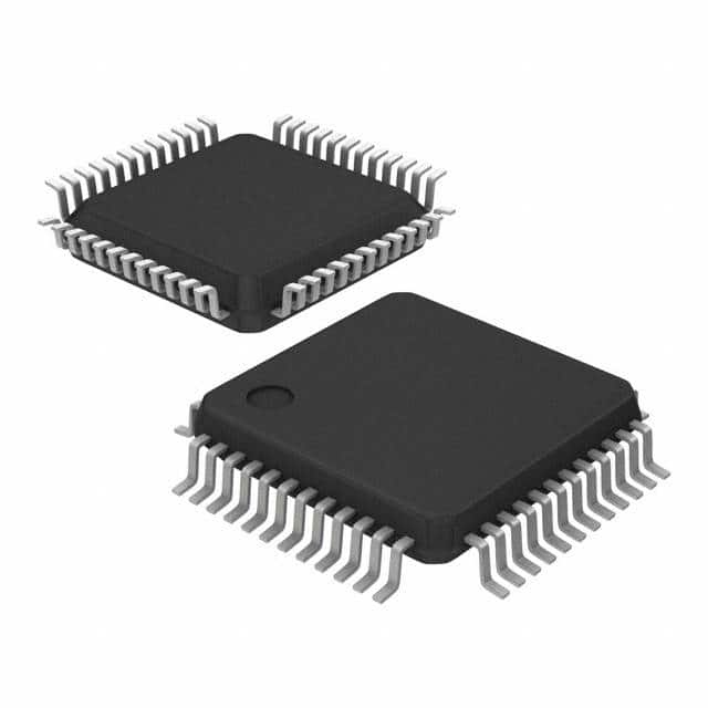
- Part No.:
- TM4C123GH6PMIR
- Manufacturer:
- Texas Instruments
- Category:
- Microcontrollers
- Package:
- 64-LQFP
- Datasheet:
-
 TM4C123GH6PMIR.pdf
- Description:
- IC MCU 32BIT 256KB FLASH 64LQFP
- Quantity:
- Payment:

- Shipping:

Inventory:749
Please send an inquiry. Send us your inquiry, and we will respond immediately.
Product details
Overview
TM4C123GH6PMIR from Texas Instruments is an ARM Cortex-M4F-based microcontroller with 256 KB Flash, 32 KB SRAM, and integrated peripherals including USB 2.0 OTG, 8× PWM generators, 2× QEI, 2× CAN, 8× UARTs, 2× I²C, 2× SPI, and a 12-bit 1-MSPS ADC. It operates at up to 80 MHz and supports -40°C to +85°C industrial temperature range. It serves as the main control unit in motor drive firmware, industrial PLCs, and USB-connected embedded gateways.
For engineers reviewing the TM4C123GH6PMIR datasheet, TM4C123GH6PMIR pinout, TM4C123GH6PMIR application, or TM4C123GH6PMIR equivalent, key selection criteria include its integrated USB PHY, dual CAN controllers with FIFO support, hibernation module with RTC and battery-backed memory, and deterministic real-time interrupt latency under 12 clock cycles.
Technical Context
The TM4C123GH6PMIR implements a full-featured ARM Cortex-M4F core with hardware floating-point unit (FPU), 3-stage pipeline, and NVIC supporting 64 interrupt lines with configurable priority grouping. Its system-level integration includes a programmable clock tree with PLL, multiple low-power modes (sleep, deep-sleep, hibernate), and a dedicated hibernation module with external wake-up capability and 256-byte battery-backed RAM.
Peripherals are tightly coupled via the μDMA controller with 32-channel arbitration, enabling zero-CPU-overhead transfers between ADC, UART, and SRAM. The analog subsystem features four independent 12-bit ADC sample sequencers with hardware averaging and digital comparators, while the motion control suite includes two quadrature encoder interfaces and eight PWM generator blocks with fault protection inputs.
Key Specifications
| Parameter | Value and Actual Design Meaning |
|---|---|
| CPU Core | ARM Cortex-M4F @ 80 MHz with FPU and 32-bit SIMD instructions for real-time signal processing |
| Memory | 256 KB on-chip Flash (with ECC), 32 KB SRAM, 2 KB EEPROM, plus 256 B hibernate RAM |
| ADC | 12-bit, 1-MSPS SAR ADC with 4 independent sample sequencers and hardware averaging up to 64x |
| Communication | 2× CAN 2.0A/B controllers, 8× UARTs (1 with IrDA/ISO7816), 2× I²C, 2× SPI, USB 2.0 OTG with integrated PHY |
| PWM & Motion | 8× PWM generator blocks (16 PWM outputs), 2× QEI modules, and fault pin support for motor control safety |
| Power Modes | Active, Sleep, Deep-Sleep, Hibernate with RTC and battery-backed memory; wake-up latency < 5 µs from hibernate |
| Temperature Range | -40°C to +85°C industrial grade, qualified per AEC-Q100 Grade 3 (not automotive) |
Pinout & Package
TM4C123GH6PMIR is housed in a 64-pin LQFP package (10 mm × 10 mm, 0.5 mm pitch) with exposed thermal pad. Pin functions are defined across five GPIO ports (A–E), plus dedicated peripheral pins for USB, CAN, UART, I²C, SPI, ADC, PWM, QEI, and debug interfaces.
| Pin/Terminal | Circuit Role | Design Meaning |
|---|---|---|
| VDD, VDDA, VDDC | Power supply inputs | VDD = 3.3 V digital core; VDDA = 3.3 V analog domain; VDDC = 1.2 V internal regulator input |
| VSS, VSSA, VSSC | Ground returns | Separate digital, analog, and core ground planes required for noise isolation and ADC accuracy |
| USB0VBUS, USB0ID, USB0DM, USB0DP | USB 2.0 OTG interface | Integrated PHY eliminates need for external transceiver; ID pin enables host/peripheral role detection |
| CAN0RX, CAN0TX, CAN1RX, CAN1TX | CAN bus transceiver I/O | Dual independent CAN controllers with message objects, FIFOs, and loopback self-test mode |
| U0RX, U0TX, U1RX, U1TX, ..., U7RX, U7TX | UART serial I/O | 8 UARTs mapped across GPIO pins; UART0 supports IrDA modulation and ISO 7816 smart card protocol |
| SSI0CLK, SSI0FSS, SSI0RX, SSI0TX | SPI master/slave interface | 2× SSI modules compatible with Motorola SPI, TI SSP, and National Microwire protocols |
| I2C0SCL, I2C0SDA, I2C1SCL, I2C1SDA | I²C bus interface | Two I²C modules with 400 kHz fast-mode support, slew-rate control, and glitch filtering |
| ADC0, ADC1, ..., ADC11 | Analog input channels | 12 single-ended or 6 differential ADC inputs routed from GPIO pins; internal temp sensor available |
| PH0, PH1, PH2, PH3 | PWM output terminals | Eight PWM generator blocks provide 16 PWM outputs; PH0–PH3 map to PWM0 outputs with dead-band and fault handling |
| JTAG/SWD | Debug interface | SWDIO, SWCLK, nSRST, and TCK/TMS/TDI/TDO support both JTAG and ARM Serial Wire Debug |
Key Features
| Feature | Design Value |
|---|---|
| Hibernation Module | Enables sub-5 µA power draw with RTC running, battery-backed 256 B RAM, and external wake-up via GPIO or RTC alarm |
| μDMA Controller | 32-channel arbiter with scatter-gather support eliminates CPU overhead for ADC-to-memory or UART-to-SRAM transfers |
| Dual CAN Controllers | Each supports 32 message objects, transmit/receive FIFOs, and automatic retransmission - critical for industrial fieldbus redundancy |
| USB 2.0 OTG with PHY | On-die USB transceiver removes need for external PHY; supports device, host, and OTG roles without external level shifters |
| Quadrature Encoder Interface | Two independent QEI modules decode position/speed from incremental encoders with direction, index, and error detection |
| Programmable Clock System | Multiple clock sources (PIOSC, MOSC, HSE, PLL) with dynamic switching and fractional dividers for precise peripheral timing |
Applications
| Industrial Motor Control | USB-Enabled Field Gateway |
|---|---|
Use Scenario: Closed-loop BLDC motor control in HVAC blowers with current sensing, position feedback, and thermal monitoring. IC Role / Device Role / Timing Role: Main system controller executing FOC algorithm, managing PWM generation, reading ADC current samples, and communicating status over CAN. Use Value: Integrated QEI, 16-channel PWM with fault protection, and deterministic 80 MHz interrupt response enable precise torque ripple reduction and safe shutdown. | Use Scenario: Protocol translation gateway connecting Modbus RTU sensors to cloud via USB CDC ACM to host PC or USB-to-Ethernet bridge. IC Role / Device Role / Timing Role: USB device controller with UART-to-USB bridging firmware, managing buffer management, flow control, and error recovery. Use Value: On-chip USB PHY and 8 kB USB packet RAM eliminate external transceiver; dual CAN allows local fieldbus aggregation before upstream upload. |
| Smart Building Sensor Node | Programmable Logic Controller (PLC) I/O Module |
Use Scenario: Battery-powered occupancy/lighting sensor node with PIR, ambient light, and temperature sensing, transmitting data hourly via USB or UART to concentrator. IC Role / Device Role / Timing Role: Low-power system manager entering hibernate between readings, waking on RTC alarm or GPIO event, and performing ADC conversions. Use Value: Sub-5 µA hibernate current with RTC and 256 B battery-backed RAM preserves state across power loss; internal temp sensor reduces BOM count. | Use Scenario: DIN-rail mounted I/O expansion module accepting 24 V DC digital inputs and driving relay outputs, communicating with main PLC over CAN or RS-485. IC Role / Device Role / Timing Role: Real-time I/O processor handling debounce, edge detection, pulse width measurement, and CAN message framing. Use Value: Eight general-purpose timers with capture/compare and PWM modes support precise timing of input pulses and output waveforms; GPIO commit registers prevent spurious output transitions during config. |
Equivalent & Alternatives
The following parts are listed as comparable options for similar microcontroller applications.
| Alternative Part | Technical Difference | Application Difference | Selection Advice |
|---|---|---|---|
| TM4C123GE6PM | Same die, but in 128-pin TQFP package with additional GPIOs, extra UART/I²C/SSI, and no USB PHY | Lacks integrated USB transceiver; requires external PHY for USB connectivity | Select when more I/O, larger memory footprint, or absence of USB is acceptable |
| STM32F407VGT6 | ARM Cortex-M4F @ 168 MHz, 1 MB Flash, 192 KB SRAM, no integrated USB PHY, no hibernation module, different peripheral set | No native hibernate mode with RTC/battery RAM; USB requires external PHY or uses USB FS-only stack | Select when higher CPU performance and larger memory are prioritized over ultra-low-power hibernate and USB integration |
Compared with TM4C123GE6PM and STM32F407VGT6, the TM4C123GH6PMIR uniquely combines USB 2.0 OTG with integrated PHY, industrial-grade hibernation with RTC and battery-backed RAM, and dual CAN in a compact 64-pin LQFP - making it optimal for space-constrained, USB-connected, low-power industrial endpoints.
Availability
TM4C123GH6PMIR is available at Aetrix Electronics and suitable for industrial motor drives, USB field gateways, and smart building sensor nodes requiring stable component supply, long-term lifecycle assurance, and traceable sourcing.
Supply support for TM4C123GH6PMIR includes scheduled delivery planning, volume procurement assistance, BOM continuity management, traceable sourcing, and lifecycle availability coordination for OEM customers, industrial embedded developers, connected-device designers, and electronics production programs.
Manufacturer
Texas Instruments is a global semiconductor company headquartered in Dallas, Texas, delivering analog, embedded processing, and wireless technologies for industrial, automotive, and consumer markets.
The TM4C123 family targets cost-sensitive, real-time industrial control applications - emphasizing integrated connectivity (USB, CAN), low-power operation, and robust peripheral sets for deterministic embedded firmware execution.
FAQ
What is the maximum operating frequency of the TM4C123GH6PMIR?
The TM4C123GH6PMIR operates at a maximum system clock frequency of 80 MHz, achieved using its internal PLL with an external crystal (4–25 MHz) or precision internal oscillator. This frequency applies to the Cortex-M4F core, bus matrix, and all synchronous peripherals. The device maintains full specification compliance-including ADC sampling rate, UART baud accuracy, and PWM resolution-at this speed across the full -40°C to +85°C temperature range.
Does the TM4C123GH6PMIR include an integrated USB physical layer (PHY)?
Yes, the TM4C123GH6PMIR integrates a full-speed USB 2.0 OTG physical layer, including differential transceivers, voltage regulators, and pull-up/pull-down resistors. This eliminates the need for an external USB PHY chip and simplifies board layout. The USB module supports device, host, and OTG roles and is accessible via dedicated pins (USB0VBUS, USB0ID, USB0DM, USB0DP) on the 64-pin LQFP package.
How does the hibernation mode function in the TM4C123GH6PMIR?
The TM4C123GH6PMIR's hibernation module reduces current consumption to under 5 µA while maintaining RTC operation and preserving 256 bytes of battery-backed RAM. It supports wake-up via RTC alarm, external GPIO interrupt, or HIB pin assertion. The module includes dedicated clock sources (hibernate RTC oscillator), battery switchover circuitry, and tamper detection - enabling reliable operation in battery-backed industrial logging and remote sensor applications.
What are the key differences between TM4C123GH6PMIR and TM4C123GH6PZ?
The TM4C123GH6PMIR and TM4C123GH6PZ share identical silicon functionality and electrical specifications but differ only in packaging and marking: TM4C123GH6PMIR uses a 64-pin LQFP with moisture sensitivity level (MSL) 3 and tape-and-reel packaging for automated assembly, while TM4C123GH6PZ uses a 100-pin TQFP. Both operate from -40°C to +85°C and support the same peripheral set, clocking, and firmware binaries.
Can the TM4C123GH6PMIR support simultaneous dual CAN communication?
Yes, the TM4C123GH6PMIR integrates two independent CAN 2.0A/B controllers (CAN0 and CAN1), each with 32 message objects, dedicated transmit/receive FIFOs, and programmable bit timing. They operate concurrently without resource contention, enabling applications such as redundant fieldbus links or hybrid networks where one CAN port handles motor control and the other manages diagnostics or sensor aggregation.
TM4C123GH6PMIR Specifications
- Product attributes
- Attribute value
- Manufacturer:
- Texas Instruments
- Package/Case:
- 64-LQFP
- Series:
- Tiva™ C
- Packaging:
- Tape & Reel (TR)
- Product Status:
- Active
- Programmable:
- Not Verified
- Core Processor:
- ARM® Cortex®-M4F
- Core Size:
- 32-Bit Single-Core
- Speed:
- 80MHz
- Connectivity:
- CANbus, I2C, IrDA, Microwire, QEI, SPI, SSI, UART/USART, USB OTG
- Peripherals:
- Brown-out Detect/Reset, DMA, Motion PWM, POR, WDT
- Number of I/O:
- 43
- Program Memory Size:
- 256KB (256K x 8)
- Program Memory Type:
- FLASH
- EEPROM Size:
- 2K x 8
- RAM Size:
- 32K x 8
- Voltage - Supply (Vcc/Vdd):
- 1.08V ~ 3.63V
- Data Converters:
- A/D 12x12b
- Oscillator Type:
- Internal
- Operating Temperature:
- -40°C ~ 85°C (TA)
- Grade:
- -
- Qualification:
- -
- Mounting Type:
- Surface Mount
- Supplier Device Package:
TM4C123GH6PMIR FAQ
1.How can I place an order for TM4C123GH6PMIR through Aetrix?
Please submit a Request for Quotation (RFQ) for TM4C123GH6PMIR on Aetrix. Our sales agent will provide a competitive quotation and guide you through the order confirmation once you accept the terms.
2.Are the price and stock information for TM4C123GH6PMIR reliable?
The price and inventory of TM4C123GH6PMIR are updated periodically and may fluctuate due to market conditions. Stock and pricing data are typically refreshed every 24 hours. Quotation validity for TM4C123GH6PMIR is usually 5 days.
3.What payment methods are accepted for TM4C123GH6PMIR?
We accept Wire Transfer, PayPal, Credit Card, Western Union, MoneyGram, and Escrow for TM4C123GH6PMIR transactions.
Note: Certain payment methods may incur a processing fee.
4.How is shipping managed for TM4C123GH6PMIR?
TM4C123GH6PMIR orders can be shipped via leading logistics carriers, including DHL, UPS, FedEx, TNT, or Registered Mail.
Once your TM4C123GH6PMIR order is processed, you will receive an email with the shipment details and tracking number.
Note: Tracking information may take up to 24 hours to appear. Express delivery typically takes 3–5 business days.
5.How can I obtain technical support or documentation for TM4C123GH6PMIR?
For technical support, including TM4C123GH6PMIR datasheets, pinout diagrams, or application guidance, please contact our engineering support team. They can provide detailed documentation and assistance for your TM4C123GH6PMIR requirements.
6.How does Aetrix verify that TM4C123GH6PMIR is sourced from the original manufacturer or authorized distributors?
All TM4C123GH6PMIR products on Aetrix are procured from qualified distributors and authorized channels. Our dedicated quality assurance team conducts strict verification, including traceability checks and, if necessary, third-party testing. This ensures that TM4C123GH6PMIR meets industry standards.
7.What is the process for return or replacement of TM4C123GH6PMIR?
All TM4C123GH6PMIR units undergo pre-shipment inspection (PSI). If there is an issue with TM4C123GH6PMIR, returns or replacements are accepted under the following conditions:
1.Quantity discrepancies, incorrect items, or visible external defects (such as breakage or corrosion), acknowledged by Aetrix.
2.The issue is reported within 90 days of delivery.
3.The TM4C123GH6PMIR part is unused and in its original packaging.
Return procedure for TM4C123GH6PMIR:
1.Submit a request within 90 days.
2.Obtain a Return Material Authorization (RMA) from Aetrix.
TM4C123GH6PMIR Tags

-
ATTINY4-TSHR
Microchip Technology
-
ATTINY10-TSHR
Microchip Technology
-
ATTINY10-TS8R
Microchip Technology

-
ATTINY202-SSNR
Microchip Technology
-
ATTINY202-SSFR
Microchip Technology
-
ATTINY402-SSNR
Microchip Technology

-
PIC16F15213T-I/MF
Microchip Technology
-
PIC16F15213-E/MF
Microchip Technology

-
PIC10F200T-I/OT
Microchip Technology
-
ATTINY412-SSNR
Microchip Technology
-
PIC10F202T-I/OT
Microchip Technology

-
ATTINY404-SSNR
Microchip Technology
Tech Hub

A practical engineering guide to 3.3V and 5V logic compatibility, input thresholds, resistor dividers, translator ICs, MOSFET level shifting, I2C pull-ups, timing limits and power-sequencing risks.

The 74HC595 uses push-pull logic outputs, while the TPIC6B595 uses 50 V open-drain DMOS sinks for higher-power loads. This guide compares timing, current limits, 3.3 V interfacing, load wiring, thermal…

The 74HC595 converts serial data into eight stable parallel outputs. This guide covers pin functions, shift and storage timing, OE and MR behavior, drive-current limits, cascading, voltage compatibilit…

A technical comparison of level-sensitive latches and edge-triggered flip-flops, covering timing windows, setup and hold limits, master–slave operation, time borrowing, race-through, HDL inference and…

A D latch stores one bit while Enable controls when data can pass. This reference covers gate-level operation, truth tables, transparency, setup and hold timing, LE versus OE, common ICs and practical …

An SR latch stores one bit through cross-coupled feedback. This engineering reference covers NOR and NAND implementations, truth tables, forbidden-state recovery, gated operation, switch debouncing, fa…

Latch circuits retain one bit through feedback. This technical reference covers SR and D latches, truth tables, transparency, timing limits, latch-versus-flip-flop behavior, applications and common log…

An engineering guide to LED driver operation, constant-current and constant-voltage outputs, linear and switching topologies, dimming, IC selection, calculations, replacement compatibility, and fault c…

Operational amplifier guide covering op amp basics, feedback, ideal vs real op amps, common configurations, buffer circuits, offset, bias current, gain-bandwidth, slew rate, rail-to-rail limits and sel…

Jumper cables guide covering safe connection order, red and black clamp placement, final ground connection, cable gauge, length, clamp quality, copper vs CCA cables, jump starter comparison and battery…


