
 My Inquiry
 My Account


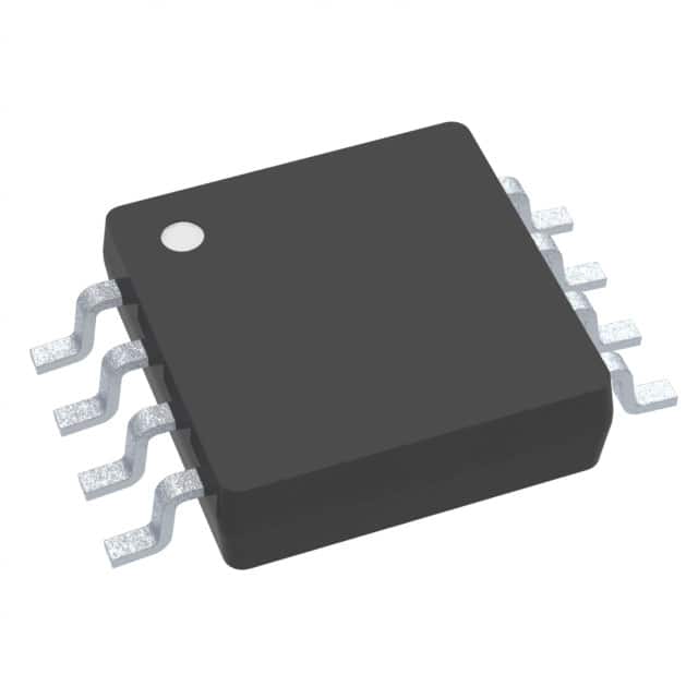
Texas Instruments TMP175AIDGKTG4
- Part No.:
- TMP175AIDGKTG4
- Manufacturer:
- Texas Instruments
- Category:
- Analog and Digital Output
- Package:
- 8-TSSOP, 8-MSOP (0.118", 3.00mm Width)
- Datasheet:
-
 TMP175AIDGKTG4.pdf
- Description:
- SENSOR DIGITAL -40C-125C 8VSSOP
- Quantity:
- Payment:

- Shipping:

Inventory:4,028
Please send an inquiry. Send us your inquiry, and we will respond immediately.
Product details
Overview
TMP175AIDGKTG4 from Texas Instruments is a digital temperature sensor with I²C/SMBus interface, designed for precision thermal monitoring in embedded systems. It delivers ±1 °C typical accuracy from −40 °C to +125 °C, 9–12-bit user-selectable resolution (down to 0.0625 °C), and operates from 2.7 V to 5.5 V. Its 8-pin VSSOP package supports up to 27 devices on one bus-ideal for multi-zone thermal management in space-constrained applications like notebook computers and battery packs.
For engineers reviewing the TMP175AIDGKTG4 datasheet, TMP175AIDGKTG4 pinout, TMP175AIDGKTG4 application, or TMP175AIDGKTG4 equivalent, key selection criteria include its 27-device addressability, SMBus Alert functionality, low 50-μA quiescent current, standby mode (0.1 μA), and compatibility with LM75-form-factor layouts-critical for drop-in thermal sensing upgrades in industrial and consumer designs.
Technical Context
The TMP175AIDGKTG4 integrates a ΔΣ ADC, on-chip oscillator, and digital control logic to convert die temperature directly into calibrated 12-bit digital output without external signal conditioning. Its internal diode-based sensor provides linear response across −40 °C to +125 °C, eliminating lookup tables or polynomial compensation.
It implements full SMBus 2.0 and I²C protocol compliance-including START/STOP, repeated START, ACK/NACK, general call, and high-speed mode (up to 2 MHz)-with integrated Schmitt-trigger inputs and spike suppression filters on SDA/SCL. The ALERT pin supports interrupt-driven thermal event detection via SMBus Alert command (0x19) with slave-address return and THIGH/TLOW status encoding.
Key Specifications
| Parameter | Value and Actual Design Meaning |
|---|---|
| Accuracy | ±1 °C (typical), ±2 °C (max) over −40 °C to +125 °C - enables reliable thermal protection without system-level calibration. |
| Resolution | 9–12 bits, user-selectable - yields 0.5 °C (9-bit) to 0.0625 °C (12-bit) step size for flexible trade-off between update rate and precision. |
| Supply Range | 2.7 V to 5.5 V - interoperates with 3.3 V and 5 V logic domains without level-shifting. |
| Quiescent Current | 50 μA (active, bus idle) - minimizes power impact in always-on thermal monitoring nodes. |
| Standby Current | 0.1 μA - extends battery life in portable devices during thermal sleep modes. |
| Address Options | 27 unique I²C addresses via A0/A1/A2 pin combinations - supports dense multi-sensor networks on single bus. |
| Interface Speed | Up to 2 MHz (high-speed mode) - reduces measurement latency in real-time thermal control loops. |
Pinout & Package
Package: 8-pin VSSOP (DGK), body size 3.00 mm × 3.00 mm, industry-standard LM75 footprint compatible with SOIC-8 PCB layouts.
| Pin/Terminal | Circuit Role | Design Meaning |
|---|---|---|
| 1 (SDA) | Serial data I/O | Open-drain bidirectional line; requires external pull-up; handles address, command, and temperature data transfer. |
| 2 (SCL) | Serial clock input | Open-drain clock line; master-generated; synchronizes all I²C transactions including configuration writes and temperature reads. |
| 3 (ALERT) | Interrupt output | Open-drain active-low alert; asserts when temperature exceeds THIGH or falls below TLOW; supports SMBus Alert protocol. |
| 4 (GND) | Ground reference | Primary return path for analog sensor core and digital interface; must be low-impedance for accuracy. |
| 5 (A2) | Address select input | Logic input determining MSB of 7-bit slave address; floating allowed (enables 27-address mode unique to TMP175). |
| 6 (A1) | Address select input | Mid-bit address select; sampled at bus start; enables unique addressing without external hardware. |
| 7 (A0) | Address select input | LSB address select; combined with A1/A2, defines full 7-bit slave address per Table 7-2 in datasheet. |
| 8 (V+) | Power supply | Single 2.7–5.5 V rail powering both analog sensor and digital interface; bypass capacitor required (0.01 μF recommended). |
Key Features
| Feature | Design Value |
|---|---|
| 27-device I²C addressability | Enables scalable thermal monitoring across complex PCBs or multi-board systems without address conflicts or bus segmentation. |
| SMBus Alert with address return | Allows host MCU to identify which sensor triggered an overtemperature event in multi-sensor configurations-reducing polling overhead and latency. |
| User-selectable 9–12-bit resolution | Permits dynamic adjustment of conversion time (27.5 ms to 300 ms) and precision to match application timing and accuracy requirements. |
| 0.1 μA shutdown current | Supports ultra-low-power wake-on-temperature designs in battery-powered IoT endpoints and wearables. |
| LM75 form factor and pinout | Enables direct replacement of legacy LM75 sensors without PCB redesign-accelerating thermal subsystem upgrades. |
Applications
| Computer Peripheral Thermal Protection | Notebook Computers |
|---|---|
Use Scenario: Real-time monitoring of GPU, chipset, or SSD temperature in desktop add-in cards and docking stations. IC Role / Device Role / Timing Role: Primary temperature sensor feeding thermal throttling logic in host firmware or EC controller. Use Value: Prevents thermal shutdown by triggering fan ramp-up or performance scaling before critical junction temperatures are reached. |
Use Scenario: Zone-based thermal sensing across CPU, battery, keyboard, and display hinge in clamshell laptops. IC Role / Device Role / Timing Role: Distributed temperature node communicating via shared I²C bus to embedded controller (EC). Use Value: Enables adaptive thermal management policies that balance performance, acoustics, and battery runtime. |
| Battery Management | Office Machines |
Use Scenario: Monitoring Li-ion battery pack temperature during charge/discharge cycles in portable power tools or medical devices. IC Role / Device Role / Timing Role: Safety-critical sensor interfacing with battery management IC (BMS) or microcontroller over I²C. Use Value: Ensures charge termination and discharge cutoff within JEITA-compliant temperature windows-preventing fire risk and capacity loss. |
Use Scenario: Thermal supervision of fuser assemblies, motors, and power supplies in laser printers and multifunction copiers. IC Role / Device Role / Timing Role: Standalone thermal monitor providing ALERT-driven shutdown signals to main controller. Use Value: Extends consumable life and prevents paper jams by maintaining optimal operating temperature in high-duty-cycle environments. |
Equivalent & Alternatives
The following parts are listed as comparable options for similar digital temperature sensing applications.
| Alternative Part | Technical Difference | Application Difference | Selection Advice |
|---|---|---|---|
| LM75BIMM/NOPB | 8-address limit (A0–A2 only), no floating-pin support; ±2 °C max accuracy; 100 μA typical supply current. | Limited to ≤8 sensors per bus; less suitable for dense thermal mapping; lacks SMBus Alert address-return capability. | Preferred for cost-sensitive, low-channel-count applications where LM75 compatibility is mandatory and 27-address scalability is unnecessary. |
| STTS751-2DMR | 16-bit resolution, ±0.5 °C max accuracy, 3.3 V-only supply (2.7–3.6 V), 12-address limit, no floating A-pins. | Higher precision but narrower voltage range; incompatible with 5 V systems; fewer address options restrict scalability. | Chosen when sub-0.5 °C accuracy is required and system operates exclusively at 3.3 V-e.g., high-end instrumentation or lab equipment. |
Compared with LM75BIMM/NOPB and STTS751-2DMR, TMP175AIDGKTG4 uniquely balances wide supply range (2.7–5.5 V), 27-address flexibility, and SMBus Alert intelligence-making it optimal for scalable, mixed-voltage thermal architectures where bus efficiency and diagnostic clarity are prioritized over marginal accuracy gains.
Availability
TMP175AIDGKTG4 is available at Aetrix Electronics and suitable for notebook computers, battery management systems, and office machines requiring stable component supply, long-term manufacturability, and LM75-pin-compatible thermal sensing solutions.
Supply support for TMP175AIDGKTG4 includes scheduled delivery planning, volume procurement assistance, BOM continuity management, traceable sourcing, and lifecycle availability coordination for OEM customers, industrial embedded developers, connected-device designers, and electronics production programs.
Manufacturer
Texas Instruments is a global semiconductor leader specializing in analog, embedded processing, and connectivity technologies, with decades of expertise in precision sensing and industrial-grade IC design.
The TMP175AIDGKTG4 belongs to TI's TMPx75 family of digital temperature sensors, engineered specifically for replacing NTC/PTC thermistors in thermal protection, environmental monitoring, and power-system management applications-delivering calibrated digital output without external components.
FAQ
What is the maximum number of TMP175AIDGKTG4 devices supported on a single I²C bus?
The TMP175AIDGKTG4 supports up to 27 unique slave addresses using its three address pins (A0, A1, A2), with floating pin states enabled. This allows 27 individual TMP175AIDGKTG4 sensors to coexist on one I²C bus without address conflict-significantly exceeding the 8-device limit of the TMP75 or LM75. Each device's address is latched at bus communication startup, ensuring deterministic operation.
Does TMP175AIDGKTG4 require external calibration to achieve ±1 °C accuracy?
No, the TMP175AIDGKTG4 achieves ±1 °C typical accuracy from −40 °C to +125 °C without factory or system-level calibration. Its on-die temperature sensor and 12-bit ΔΣ ADC are trimmed during production, delivering linear, digitally compensated output. Users read raw temperature data directly from the register-no lookup tables, polynomials, or external components are needed to meet this specification.
How does the SMBus Alert function work on TMP175AIDGKTG4?
When configured in interrupt mode (TM = 1), the TMP175AIDGKTG4 asserts its open-drain ALERT pin low upon crossing THIGH or falling below TLOW. A master issuing the SMBus Alert command (0x19) receives the TMP175AIDGKTG4's slave address back on SDA, with the LSB indicating cause (high = THIGH breach, low = TLOW breach). This enables rapid identification of the triggering sensor in multi-node systems.
What is the minimum I²C clock frequency to avoid timeout on TMP175AIDGKTG4?
The TMP175AIDGKTG4 features a serial interface timeout that resets the device if SCL or SDA remains low for >54 ms (typical) between START and STOP. To prevent spurious resets, the SCL operating frequency must remain ≥1 kHz during active communication. This ensures robust operation even under low-speed debug or slow microcontroller I²C implementations.
Is TMP175AIDGKTG4 pin-compatible with standard LM75 footprints?
Yes, the TMP175AIDGKTG4 in DGK (VSSOP-8) package shares identical pinout, spacing, and mechanical dimensions with the industry-standard LM75 SOIC-8 and MSOP-8 variants. Its pin 1 orientation, terminal functions (SDA, SCL, ALERT, GND, A0–A2, V+), and LM75-equivalent footprint allow direct PCB-level replacement-no layout changes or rework required when upgrading from LM75-based designs.
TMP175AIDGKTG4 Specifications
- Product attributes
- Attribute value
- Manufacturer:
- Texas Instruments
- Series:
- -
- Package/Case:
- 8-TSSOP, 8-MSOP (0.118", 3.00mm Width)
- Packaging:
- Tape & Reel (TR)
- Product Status:
- Obsolete
- Sensor Type:
- Digital, Local
- Sensing Temperature - Local:
- -40°C ~ 125°C
- Sensing Temperature - Remote:
- -
- Output Type:
- I2C/SMBus
- Voltage - Supply:
- 2.7V ~ 5.5V
- Resolution:
- 9 b
- Features:
- One-Shot, Output Switch, Programmable Resolution, Shutdown Mode, Standby Mode
- Accuracy - Highest (Lowest):
- ±1.5°C (±2°C)
- Test Condition:
- -25°C ~ 85°C (-40°C ~ 125°C)
- Operating Temperature:
- -55°C ~ 127°C
- Mounting Type:
- Surface Mount
- Grade:
- -
- Qualification:
- -
- Supplier Device Package:
- 8-VSSOP
TMP175AIDGKTG4 FAQ
1.How can I place an order for TMP175AIDGKTG4 through Aetrix?
Please submit a Request for Quotation (RFQ) for TMP175AIDGKTG4 on Aetrix. Our sales agent will provide a competitive quotation and guide you through the order confirmation once you accept the terms.
2.Are the price and stock information for TMP175AIDGKTG4 reliable?
The price and inventory of TMP175AIDGKTG4 are updated periodically and may fluctuate due to market conditions. Stock and pricing data are typically refreshed every 24 hours. Quotation validity for TMP175AIDGKTG4 is usually 5 days.
3.What payment methods are accepted for TMP175AIDGKTG4?
We accept Wire Transfer, PayPal, Credit Card, Western Union, MoneyGram, and Escrow for TMP175AIDGKTG4 transactions.
Note: Certain payment methods may incur a processing fee.
4.How is shipping managed for TMP175AIDGKTG4?
TMP175AIDGKTG4 orders can be shipped via leading logistics carriers, including DHL, UPS, FedEx, TNT, or Registered Mail.
Once your TMP175AIDGKTG4 order is processed, you will receive an email with the shipment details and tracking number.
Note: Tracking information may take up to 24 hours to appear. Express delivery typically takes 3–5 business days.
5.How can I obtain technical support or documentation for TMP175AIDGKTG4?
For technical support, including TMP175AIDGKTG4 datasheets, pinout diagrams, or application guidance, please contact our engineering support team. They can provide detailed documentation and assistance for your TMP175AIDGKTG4 requirements.
6.How does Aetrix verify that TMP175AIDGKTG4 is sourced from the original manufacturer or authorized distributors?
All TMP175AIDGKTG4 products on Aetrix are procured from qualified distributors and authorized channels. Our dedicated quality assurance team conducts strict verification, including traceability checks and, if necessary, third-party testing. This ensures that TMP175AIDGKTG4 meets industry standards.
7.What is the process for return or replacement of TMP175AIDGKTG4?
All TMP175AIDGKTG4 units undergo pre-shipment inspection (PSI). If there is an issue with TMP175AIDGKTG4, returns or replacements are accepted under the following conditions:
1.Quantity discrepancies, incorrect items, or visible external defects (such as breakage or corrosion), acknowledged by Aetrix.
2.The issue is reported within 90 days of delivery.
3.The TMP175AIDGKTG4 part is unused and in its original packaging.
Return procedure for TMP175AIDGKTG4:
1.Submit a request within 90 days.
2.Obtain a Return Material Authorization (RMA) from Aetrix.
TMP175AIDGKTG4 Tags
-
MCP9700T-E/TT
Microchip Technology
-
MCP9700T-E/LT
Microchip Technology
-
MCP9701T-E/TT
Microchip Technology
-
MCP9701T-E/LT
Microchip Technology
-
TMP235A4DBZR
Texas Instruments
-
MCP9700AT-E/TT
Microchip Technology
-
MCP9700AT-E/LT
Microchip Technology
-
MCP9701AT-E/LT
Microchip Technology
-
MCP9701AT-E/TT
Microchip Technology
,TO-226_straightlead.jpg)
-
LM335Z
STMicroelectronics
-
TMP1075NDRLR
Texas Instruments
-
TMP1075DGKR
Texas Instruments
Tech Hub

A practical engineering guide to 3.3V and 5V logic compatibility, input thresholds, resistor dividers, translator ICs, MOSFET level shifting, I2C pull-ups, timing limits and power-sequencing risks.

The 74HC595 uses push-pull logic outputs, while the TPIC6B595 uses 50 V open-drain DMOS sinks for higher-power loads. This guide compares timing, current limits, 3.3 V interfacing, load wiring, thermal…

The 74HC595 converts serial data into eight stable parallel outputs. This guide covers pin functions, shift and storage timing, OE and MR behavior, drive-current limits, cascading, voltage compatibilit…

A technical comparison of level-sensitive latches and edge-triggered flip-flops, covering timing windows, setup and hold limits, master–slave operation, time borrowing, race-through, HDL inference and…

A D latch stores one bit while Enable controls when data can pass. This reference covers gate-level operation, truth tables, transparency, setup and hold timing, LE versus OE, common ICs and practical …

An SR latch stores one bit through cross-coupled feedback. This engineering reference covers NOR and NAND implementations, truth tables, forbidden-state recovery, gated operation, switch debouncing, fa…

Latch circuits retain one bit through feedback. This technical reference covers SR and D latches, truth tables, transparency, timing limits, latch-versus-flip-flop behavior, applications and common log…

An engineering guide to LED driver operation, constant-current and constant-voltage outputs, linear and switching topologies, dimming, IC selection, calculations, replacement compatibility, and fault c…

Operational amplifier guide covering op amp basics, feedback, ideal vs real op amps, common configurations, buffer circuits, offset, bias current, gain-bandwidth, slew rate, rail-to-rail limits and sel…

Jumper cables guide covering safe connection order, red and black clamp placement, final ground connection, cable gauge, length, clamp quality, copper vs CCA cables, jump starter comparison and battery…


