
 My Inquiry
 My Account


Texas Instruments TMS320C6418ZTS600
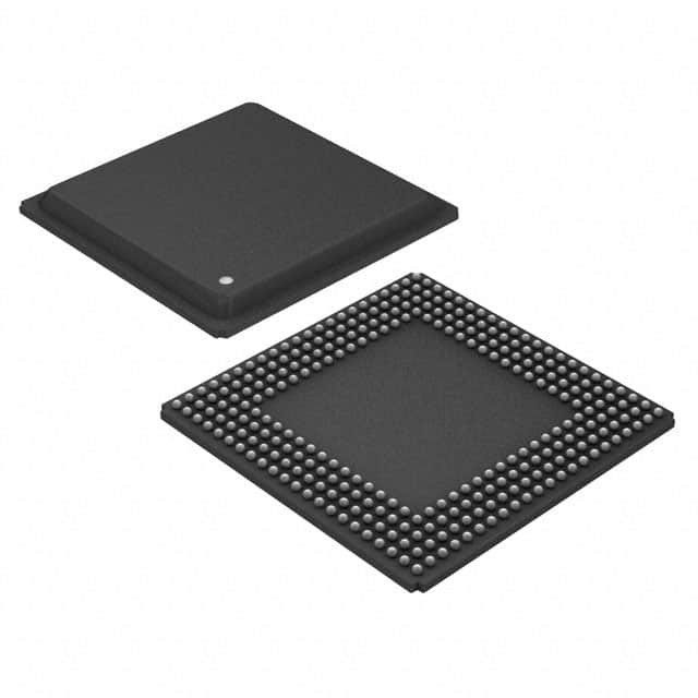
- Part No.:
- TMS320C6418ZTS600
- Manufacturer:
- Texas Instruments
- Category:
- DSP (Digital Signal Processors)
- Package:
- 288-BBGA, FCBGA
- Datasheet:
-
 TMS320C6418ZTS600.pdf
- Description:
- IC DSP FIXED-POINT 288-FCBGA
- Quantity:
- Payment:

- Shipping:

Inventory:1,115
Please send an inquiry. Send us your inquiry, and we will respond immediately.
Product details
Overview
TMS320C6418ZTS600 from Texas Instruments is a fixed-point digital signal processor (DSP) featuring a 600-MHz C64x+ CPU core, 1-MB on-chip L2 RAM/cache, 32-bit EMIFA with SDRAM/ROM support, dual McASP audio interfaces, and integrated Viterbi coprocessor. It operates at 1.2-V core voltage and 3.3-V I/O, targeting real-time telecom infrastructure, voice processing, and industrial control systems requiring deterministic low-latency signal execution.
For engineers reviewing the TMS320C6418ZTS600 datasheet, TMS320C6418ZTS600 pinout, TMS320C6418ZTS600 application, or TMS320C6418ZTS600 equivalent, key selection criteria include EMIFA timing compliance for external memory interfacing, McASP channel count and clock domain flexibility, PLL configuration options for system clock synthesis, and thermal derating within the 0°C to 90°C case temperature range.
Technical Context
The TMS320C6418ZTS600 implements an eight-way very long instruction word (VLIW) C64x+ DSP core with 64 general-purpose 32-bit registers and two 16-bit multipliers per functional unit, enabling up to 4800 MIPS peak performance. Its memory subsystem includes 64 KB L1P program cache, 64 KB L1D data cache, and configurable 1-MB L2 unified RAM/cache with programmable partitioning between SRAM and cache modes.
Peripherals are managed via a hierarchical bus architecture: the EMIFA supports asynchronous, synchronous, and SDRAM interfaces with programmable timing registers; dual McASPs provide time-division multiplexed (TDM) and I2S audio I/O with independent transmit/receive clocks; and the VCP offloads convolutional decoding tasks with dedicated Viterbi algorithm hardware.
Key Specifications
| Parameter | Value and Actual Design Meaning |
|---|---|
| CPU Core | C64x+ VLIW DSP running at 600 MHz - delivers 4800 MIPS for real-time signal processing loops without pipeline stalls. |
| L2 Memory | 1-MB on-chip unified RAM/cache - configurable as full SRAM, full cache, or split mode for deterministic latency-critical code/data placement. |
| EMIFA Width | 32-bit external memory interface - supports up to 512-MB address space with SDRAM, ROM, and asynchronous peripheral mapping. |
| McASP Count | Dual multichannel audio serial ports - each supports up to 16 TDM slots, independent bit clocks, and frame syncs for multi-channel voice or audio streaming. |
| VCP | Integrated Viterbi decoder coprocessor - accelerates convolutional decoding at up to 128 kbps, reducing CPU load in telecom baseband processing. |
| Operating Temperature | 0°C to 90°C case temperature - defines thermal design envelope for board-level heatsinking and airflow requirements in enclosed industrial enclosures. |
| Supply Voltages | DVDD = 1.2 V ± 3%, CVDD = 1.2 V, AVDD = 3.3 V, DVDDIO = 3.3 V - mandates separate low-noise LDOs and strict sequencing (DVDD/CVDD before DVDDIO). |
Pinout & Package
Package: 361-pin ZTS (Fine-Pitch Ball Grid Array), 16 mm × 16 mm, 0.8-mm pitch, RoHS-compliant, thermally enhanced with exposed thermal pad.
| Pin/Terminal | Circuit Role | Design Meaning |
|---|---|---|
| AEA[22:3] | EMIFA Address Bus | 32-bit multiplexed address lines for ROM/SDRAM access; boot mode configured via AEA[22:21] during reset. |
| ED[31:0] | EMIFA Data Bus | 32-bit bidirectional data path supporting burst reads/writes and byte-lane enables for mixed-width peripherals. |
| CLKIN | Input Clock Source | Accepts 12–30 MHz crystal or oscillator input; feeds PLL for internal 600-MHz core clock generation. |
| CLKOUT4/CLKOUT6 | Output Clock Signals | Dedicated outputs for driving external logic or ADC/DAC sampling clocks; frequency programmable via PLL dividers. |
| MCASP0_AXR0–7 | McASP0 Serial Data Lines | Eight bidirectional serial data pins supporting TDM, I2S, or custom audio protocols with independent direction control per pin. |
| VSS/VDD | Ground and Power Terminals | Multiple distributed balls for DVDD (1.2 V), CVDD (1.2 V), AVDD (3.3 V), and DVDDIO (3.3 V) ensure low-impedance return paths and noise isolation. |
Key Features
| Feature | Design Value |
|---|---|
| Configurable L2 Memory | 1-MB on-chip memory partitioned into SRAM and cache segments - enables hard real-time code execution with zero cache-miss latency guarantees. |
| EMIFA Timing Flexibility | Programmable setup/hold/wait states per memory region - allows direct interfacing with legacy NOR flash, FPGA peripherals, and DDR SDRAM without glue logic. |
| Dual Independent McASPs | Two fully autonomous audio ports with separate clock domains and DMA channels - supports simultaneous VoIP codec processing and telephony line interface I/O. |
| Viterbi Coprocessor (VCP) | Dedicated hardware accelerator for convolutional decoding - reduces CPU utilization by >90% in GSM/CDMA baseband applications versus software-only implementation. |
| Power-Down Modes | Four low-power states (IDLE, STANDBY, HALT, and DEEPSLEEP) with wake-up via GPIO, timer, or external interrupt - extends runtime in battery-backed voice recorders. |
Applications
| Voice over IP Gateway | Industrial Motor Control |
|---|---|
Use Scenario: Real-time G.729/G.723.1 speech encoding/decoding with echo cancellation and jitter buffering across multiple SIP channels. IC Role / Device Role / Timing Role: Primary DSP executing codec algorithms, managing McASP audio streams, and coordinating EMIFA-based packet buffer memory. Use Value: 4800 MIPS headroom ensures concurrent processing of 16+ voice channels with <10-ms end-to-end latency under full load. |
Use Scenario: Closed-loop field-oriented control (FOC) of three-phase AC induction motors with sensorless rotor position estimation. IC Role / Device Role / Timing Role: Real-time execution of Park/Clarke transforms, PI current regulators, and space-vector PWM generation at 20-kHz switching frequency. Use Value: Deterministic 50-ns instruction cycle enables sub-microsecond current loop response times critical for torque ripple suppression. |
| Telecom Base Station Modem | Medical Ultrasound Beamformer |
Use Scenario: Forward error correction (FEC) and channel equalization in point-to-multipoint wireless backhaul modems operating at 2 Mbps. IC Role / Device Role / Timing Role: Offloading VCP for Viterbi decoding while CPU handles adaptive equalizer coefficient updates via LMS algorithm. Use Value: Integrated VCP achieves 128-kbps convolutional decode throughput with <200-cycle latency, freeing CPU for higher-layer protocol stack tasks. |
Use Scenario: Digital beamforming of 128-channel ultrasound receive data with dynamic focusing and harmonic imaging processing. IC Role / Device Role / Timing Role: High-throughput processing of time-aligned RF samples using L2 SRAM-resident FIR filters and delay-and-sum operations. Use Value: 1-MB L2 SRAM configured as dual-port memory enables simultaneous acquisition (DMA) and processing (CPU) without contention or external DRAM bottlenecks. |
Equivalent & Alternatives
The following parts are listed as comparable options for similar fixed-point DSP applications.
| Alternative Part | Technical Difference | Application Difference | Selection Advice |
|---|---|---|---|
| TMS320C6455ZTZ600 | Higher-performance C64x+ core (1 GHz), 2-MB L2, PCI Express interface, no VCP | Targets high-throughput video analytics and radar signal processing where VCP is unnecessary but PCIe host connectivity is required | Select when system bandwidth exceeds EMIFA limits and PCIe endpoint functionality is needed; requires PCB redesign due to 529-pin ZTZ package |
| TMS320C6748ZWT6 | Floating-point C674x core (456 MHz), 256-KB L2, no VCP, ARM9 coprocessor, smaller 361-pin ZWT package | Suitable for mixed-signal applications requiring floating-point math (e.g., FFT-based spectral analysis) and lightweight OS support via ARM9 | Select when algorithmic precision demands IEEE-754 compliance and dual-core heterogeneity improves system responsiveness; lower MIPS but better numeric fidelity |
Compared with TMS320C6418ZTS600, the C6455 offers higher raw compute and PCIe I/O at the cost of larger footprint and missing VCP acceleration, while the C6748 trades fixed-point determinism and VCP for floating-point flexibility and ARM-assisted control - choice depends on whether telecom FEC offload or spectral analysis precision dominates the system's computational bottleneck.
Availability
TMS320C6418ZTS600 is available at Aetrix Electronics and suitable for voice processing gateways, industrial motor drives, and telecom modem designs requiring stable component supply, long-term lifecycle assurance, and traceable sourcing from authorized channels.
Supply support for TMS320C6418ZTS600 includes scheduled delivery planning, volume procurement assistance, BOM continuity management, traceable sourcing, and lifecycle availability coordination for OEM customers, industrial embedded developers, connected-device designers, and electronics production programs.
Manufacturer
Texas Instruments is a global semiconductor leader specializing in analog, embedded processing, and connectivity technologies, with decades of DSP innovation rooted in TI's TMS320 architecture lineage.
The TMS320C6418ZTS600 belongs to TI's C6000 fixed-point DSP product line, engineered for deterministic real-time signal processing in telecom infrastructure, voice communications, and industrial automation where MIPS efficiency and peripheral integration outweigh floating-point needs.
FAQ
What is the maximum operating frequency of the TMS320C6418ZTS600?
The TMS320C6418ZTS600 operates at a guaranteed maximum CPU clock frequency of 600 MHz across its specified case temperature range of 0°C to 90°C. This frequency is achieved using the on-chip PLL with appropriate input clock and divider settings; exceeding 600 MHz violates production specifications and may cause timing violations or functional failure in the TMS320C6418ZTS600.
Does the TMS320C6418ZTS600 support JTAG debugging?
Yes, the TMS320C6418ZTS600 fully supports IEEE 1149.1 JTAG boundary-scan and emulation via dedicated TCK, TMS, TDI, TDO, and TRST pins. The device includes a JTAG ID register (value 0x0007902F) and supports real-time tracing, breakpoint insertion, and memory/register access during active execution - essential for development and validation of complex TMS320C6418ZTS600-based systems.
Can the TMS320C6418ZTS600 boot directly from external SDRAM?
No, the TMS320C6418ZTS600 does not support booting directly from SDRAM. Boot modes are selected via AEA[22:19] pins at reset and include options such as EMIFA 8-bit ROM boot, HPI boot, or no-boot (internal ROM). SDRAM initialization must be performed by boot code loaded from ROM or external flash before the TMS320C6418ZTS600 can execute from SDRAM.
What power supply sequencing is required for reliable TMS320C6418ZTS600 operation?
The TMS320C6418ZTS600 requires strict power supply sequencing: DVDD and CVDD (1.2 V) must be stable before DVDDIO (3.3 V) ramps up. Violating this sequence risks latch-up or undefined reset behavior. TI recommends using sequenced LDOs or a dedicated power-management IC to enforce the correct ramp order and hold times for all four supply domains in the TMS320C6418ZTS600.
How many independent clock domains does the TMS320C6418ZTS600 support for McASP peripherals?
The TMS320C6418ZTS600 supports two fully independent clock domains for its dual McASP modules: McASP0 and McASP1 each have dedicated ACLKX, ACLKR, AHCLKX, and AHCLKR inputs, allowing simultaneous operation at different sample rates (e.g., 8 kHz for telephony and 48 kHz for audio monitoring) without cross-domain synchronization overhead in the TMS320C6418ZTS600.
TMS320C6418ZTS600 Specifications
- Product attributes
- Attribute value
- Manufacturer:
- Texas Instruments
- Series:
- TMS320C6410/12/13/18
- Package/Case:
- 288-BBGA, FCBGA
- Packaging:
- Tube
- Product Status:
- Active
- Type:
- Fixed Point
- Interface:
- Host Interface, I2C, McASP, McBSP
- Clock Rate:
- 600MHz
- Non-Volatile Memory:
- External
- On-Chip RAM:
- 544kB
- Voltage - I/O:
- 3.30V
- Voltage - Core:
- 1.40V
- Operating Temperature:
- 0°C ~ 90°C (TC)
- Grade:
- -
- Qualification:
- -
- Mounting Type:
- Surface Mount
- Supplier Device Package:
- 288-FCBGA (23x23)
TMS320C6418ZTS600 FAQ
1.How can I place an order for TMS320C6418ZTS600 through Aetrix?
Please submit a Request for Quotation (RFQ) for TMS320C6418ZTS600 on Aetrix. Our sales agent will provide a competitive quotation and guide you through the order confirmation once you accept the terms.
2.Are the price and stock information for TMS320C6418ZTS600 reliable?
The price and inventory of TMS320C6418ZTS600 are updated periodically and may fluctuate due to market conditions. Stock and pricing data are typically refreshed every 24 hours. Quotation validity for TMS320C6418ZTS600 is usually 5 days.
3.What payment methods are accepted for TMS320C6418ZTS600?
We accept Wire Transfer, PayPal, Credit Card, Western Union, MoneyGram, and Escrow for TMS320C6418ZTS600 transactions.
Note: Certain payment methods may incur a processing fee.
4.How is shipping managed for TMS320C6418ZTS600?
TMS320C6418ZTS600 orders can be shipped via leading logistics carriers, including DHL, UPS, FedEx, TNT, or Registered Mail.
Once your TMS320C6418ZTS600 order is processed, you will receive an email with the shipment details and tracking number.
Note: Tracking information may take up to 24 hours to appear. Express delivery typically takes 3–5 business days.
5.How can I obtain technical support or documentation for TMS320C6418ZTS600?
For technical support, including TMS320C6418ZTS600 datasheets, pinout diagrams, or application guidance, please contact our engineering support team. They can provide detailed documentation and assistance for your TMS320C6418ZTS600 requirements.
6.How does Aetrix verify that TMS320C6418ZTS600 is sourced from the original manufacturer or authorized distributors?
All TMS320C6418ZTS600 products on Aetrix are procured from qualified distributors and authorized channels. Our dedicated quality assurance team conducts strict verification, including traceability checks and, if necessary, third-party testing. This ensures that TMS320C6418ZTS600 meets industry standards.
7.What is the process for return or replacement of TMS320C6418ZTS600?
All TMS320C6418ZTS600 units undergo pre-shipment inspection (PSI). If there is an issue with TMS320C6418ZTS600, returns or replacements are accepted under the following conditions:
1.Quantity discrepancies, incorrect items, or visible external defects (such as breakage or corrosion), acknowledged by Aetrix.
2.The issue is reported within 90 days of delivery.
3.The TMS320C6418ZTS600 part is unused and in its original packaging.
Return procedure for TMS320C6418ZTS600:
1.Submit a request within 90 days.
2.Obtain a Return Material Authorization (RMA) from Aetrix.
TMS320C6418ZTS600 Tags
-
TMS320C5535AZAY10
Texas Instruments
-
TMS320VC5501PGF300
Texas Instruments
-
ADSP-BF592KCPZ
Analog Devices Inc.
-
ADAU1463WBCPZ150
Analog Devices Inc.

-
TMS320VC5402PGE100
Texas Instruments

-
ADAU1701JSTZ-RL
Analog Devices Inc.
-
ADAU1701JSTZ
Analog Devices Inc.
-
TMS320VC5502PGF300
Texas Instruments
-
ADAU1462WBCPZ300RL
Analog Devices Inc.
-
ADAU1452KCPZRL
Analog Devices Inc.
-
ADAU1452WBCPZ-RL
Analog Devices Inc.
-
TMS320C6747DZKB3
Texas Instruments
Tech Hub

A practical engineering guide to 3.3V and 5V logic compatibility, input thresholds, resistor dividers, translator ICs, MOSFET level shifting, I2C pull-ups, timing limits and power-sequencing risks.

The 74HC595 uses push-pull logic outputs, while the TPIC6B595 uses 50 V open-drain DMOS sinks for higher-power loads. This guide compares timing, current limits, 3.3 V interfacing, load wiring, thermal…

The 74HC595 converts serial data into eight stable parallel outputs. This guide covers pin functions, shift and storage timing, OE and MR behavior, drive-current limits, cascading, voltage compatibilit…

A technical comparison of level-sensitive latches and edge-triggered flip-flops, covering timing windows, setup and hold limits, master–slave operation, time borrowing, race-through, HDL inference and…

A D latch stores one bit while Enable controls when data can pass. This reference covers gate-level operation, truth tables, transparency, setup and hold timing, LE versus OE, common ICs and practical …

An SR latch stores one bit through cross-coupled feedback. This engineering reference covers NOR and NAND implementations, truth tables, forbidden-state recovery, gated operation, switch debouncing, fa…

Latch circuits retain one bit through feedback. This technical reference covers SR and D latches, truth tables, transparency, timing limits, latch-versus-flip-flop behavior, applications and common log…

An engineering guide to LED driver operation, constant-current and constant-voltage outputs, linear and switching topologies, dimming, IC selection, calculations, replacement compatibility, and fault c…

Operational amplifier guide covering op amp basics, feedback, ideal vs real op amps, common configurations, buffer circuits, offset, bias current, gain-bandwidth, slew rate, rail-to-rail limits and sel…

Jumper cables guide covering safe connection order, red and black clamp placement, final ground connection, cable gauge, length, clamp quality, copper vs CCA cables, jump starter comparison and battery…


