
 My Inquiry
 My Account


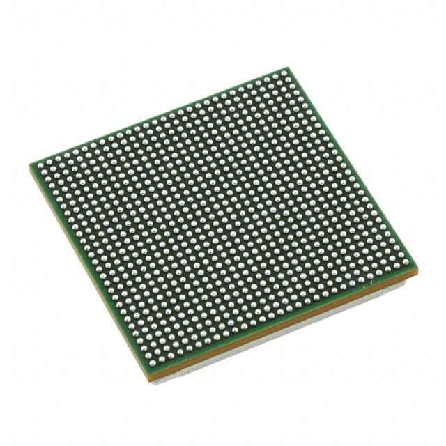
Texas Instruments TMS320C6678CYPA
- Part No.:
- TMS320C6678CYPA
- Manufacturer:
- Texas Instruments
- Category:
- DSP (Digital Signal Processors)
- Package:
- 841-BFBGA, FCBGA
- Datasheet:
-
 TMS320C6678CYPA.pdf
- Description:
- IC DSP FIX/FLOAT POINT 841FCBGA
- Quantity:
- Payment:

- Shipping:

Inventory:2,328
Please send an inquiry. Send us your inquiry, and we will respond immediately.
Product details
Overview
TMS320C6678CYPA from Texas Instruments is an eight-core fixed- and floating-point digital signal processor based on the KeyStone multicore architecture, operating at up to 1.4 GHz per core with 44.8 GMAC/core (fixed-point) and 22.4 GFLOP/core (floating-point). It integrates 4 MB of shared MSM SRAM, a 64-bit DDR3-1600 interface, and hardware accelerators for packet and security processing. This device serves as the computational engine in high-throughput communications infrastructure equipment such as wireless baseband units and packet gateways.
For engineers reviewing the TMS320C6678CYPA datasheet, TMS320C6678CYPA pinout, TMS320C6678CYPA application, or TMS320C6678CYPA equivalent, key selection criteria include per-core computational throughput, integrated network coprocessor support for IPsec/GTP-U/PDCP, MSM memory coherency model, HyperLink inter-chip scalability, and compatibility with TI's C6000 software ecosystem.
Technical Context
The TMS320C6678CYPA implements TI's KeyStone architecture centered on four hardware pillars: the Multicore Navigator for 8192-hardware-queue packet dispatch, the non-blocking TeraNet switch fabric for 2-Tbps internal bandwidth, the Multicore Shared Memory Controller (MSMC) managing 4 MB of error-correcting MSM SRAM, and HyperLink enabling 50-Gbaud chip-to-chip interconnect. All eight C66x CorePacs share access to MSM SRAM and DDR3 EMIF via dedicated memory protection units.
Its network coprocessor contains two independent engines: a packet accelerator supporting transport-layer protocols (IPsec, GTP-U, SCTP, PDCP) at 1.5 Mpackets/s wire-speed, and a security accelerator delivering up to 2.8 Gbps encryption across AES, SHA-2, HMAC, and 3GPP-compliant algorithms. The device supports boot from PCIe, SRIO, I²C, SPI, or HyperLink, with configurable PLLs (MAIN, DDR3, PASS) and SmartReflex dynamic voltage scaling.
Key Specifications
| Parameter | Value and Actual Design Meaning |
|---|---|
| Core Count & Type | Eight C66x DSP cores, each capable of 1.4 GHz fixed/floating-point operation with IEEE 754 compliance and backward code compatibility with C6000 family. |
| Computational Throughput | 44.8 GMAC/core and 22.4 GFLOP/core at 1.4 GHz - enables real-time baseband processing for multi-carrier LTE-A and 5G NR physical layer stacks. |
| On-Chip Memory | 32 KB L1P + 32 KB L1D + 512 KB L2 per core; 4096 KB MSM SRAM shared across all cores with ECC and memory protection unit. |
| External Memory Interface | 64-bit DDR3-1600 EMIF supporting up to 8 GB addressable space with ECC DRAM support for system reliability. |
| High-Speed Interconnects | Four-lane SRIO 2.1 (up to 5 GBaud/lane), PCIe Gen2 x2, HyperLink (50 Gbaud full-duplex), dual SGMII Gigabit Ethernet ports. |
| Accelerators | Packet Accelerator (1.5 Mpackets/s, L2–L4 classification, checksum, QoS) and Security Accelerator (AES/SHA/ECB/CBC/CTR/GCM/HMAC up to 2.8 Gbps). |
| Temperature Range | Extended industrial range: –40°C to +100°C - qualified for deployment in outdoor macrocell and remote radio head environments. |
Pinout & Package
The TMS320C6678CYPA is housed in a 841-pin FCCSP (Fine-Pitch Chip Scale Package) with 0.8 mm pitch, thermally enhanced for high-power multicore operation. Package dimensions are 27 mm × 27 mm × 1.2 mm (height), with exposed thermal pad on underside.
| Pin/Terminal | Circuit Role | Design Meaning |
|---|---|---|
| CLKIN | Main oscillator input | Accepts differential 100 MHz reference clock for MAIN PLL; required for synchronous boot and timing domain initialization. |
| DDR3_DQ[63:0] | DDR3 data bus | 64-bit bidirectional data interface to DDR3 SDRAM; supports burst transfers aligned to 64-byte cache lines for L3 access efficiency. |
| SRIO_LANE[3:0]_N/P | RapidIO differential lanes | Four independent 5 GBaud differential pairs supporting direct I/O and message passing; used for inter-processor communication in distributed baseband systems. |
| HYPERLINK_TX/RX[3:0]_N/P | HyperLink transceivers | Four full-duplex 12.5 Gbaud differential lanes enabling chip-to-chip scaling with zero-software-overhead task migration across KeyStone devices. |
| SGMII_CLK[1:0] | Gigabit Ethernet reference clocks | Differential 125 MHz clocks for dual SGMII PHY interfaces; allows integration of Layer 2 switching without external MAC/PHY components. |
| BOOTMODE[3:0] | Boot configuration inputs | Strapped at power-up to select boot source (SPI, I²C, PCIe, SRIO, HyperLink); determines initial firmware load path and PLL lock sequence. |
Key Features
| Feature | Design Value |
|---|---|
| 8192-Hardware Queue Multicore Navigator | Enables zero-overhead packet-based DMA and hardware-accelerated task dispatch across all eight cores without software scheduler intervention. |
| Integrated Packet Accelerator | Offloads L2–L4 packet classification, checksum insertion/verification, and QoS tagging - reduces CPU load by >70% in LTE user-plane processing. |
| Security Accelerator with 2.8 Gbps Throughput | Hardware-accelerated encryption/decryption for IPsec, SRTP, and 3GPP air interface protocols eliminates need for external crypto ICs in secure backhaul designs. |
| Backward-Compatible C66x Core | Maintains binary compatibility with legacy C64x+/C67x software, enabling reuse of mature DSP kernels and shortening time-to-market for upgraded platforms. |
| SmartReflex Dynamic Voltage Scaling | Automatically adjusts CVDD supply voltage based on real-time workload and temperature, reducing active power by up to 25% without performance loss. |
Applications
| Wireless Baseband Processing | Secure Packet Gateway |
|---|---|
Use Scenario: Real-time execution of LTE-Advanced and 5G NR physical layer algorithms including FFT, channel estimation, LDPC decoding, and MIMO precoding across multiple carriers. IC Role / Device Role / Timing Role: Primary compute engine performing deterministic, low-latency signal processing with cycle-accurate timing control via 16 programmable 64-bit timers. Use Value: Delivers 11.2 GHz aggregate DSP performance while maintaining cache-coherent memory access across all eight cores - essential for meeting sub-100 µs frame processing deadlines. | Use Scenario: High-throughput inspection and forwarding of encrypted IP packets in carrier-grade mobile core networks (e.g., EPC, 5GC). IC Role / Device Role / Timing Role: System-on-chip platform integrating packet acceleration, security offload, and switching - replaces discrete NPU + crypto + switch ASIC combination. Use Value: Achieves 1-Gbps wire-speed IPsec/GTP-U processing using integrated accelerators, eliminating bottlenecks from PCIe bus transfer latency and host CPU scheduling jitter. |
| Radar Signal Processing | Industrial Video Analytics Edge Node |
Use Scenario: Multi-channel beamforming, pulse-Doppler processing, and CFAR detection in phased-array radar systems deployed in aerospace and defense platforms. IC Role / Device Role / Timing Role: Deterministic real-time DSP subsystem synchronized to radar chirp timing via GPIO-triggered timer capture and EDMA3-linked list transfers. Use Value: Leverages per-core L2 SRAM and MSM coherence to sustain >20 GB/s memory bandwidth for streaming ADC sample buffers and coefficient tables - critical for wideband SAR imaging. | Use Scenario: On-device inference and feature extraction from HD video streams in smart factory vision systems, including object detection, motion tracking, and anomaly classification. IC Role / Device Role / Timing Role: Heterogeneous compute node executing optimized C66x assembly kernels for convolution, optical flow, and histogram analysis alongside ARM-hosted AI frameworks. Use Value: Uses TSIP and EMIF16 interfaces to connect to FPGA-based sensor pre-processing pipelines and DDR3-based frame buffers - enabling <50 ms end-to-end latency from camera input to decision output. |
Equivalent & Alternatives
The following parts are listed as comparable options for similar multicore DSP applications.
| Alternative Part | Technical Difference | Application Difference | Selection Advice |
|---|---|---|---|
| TMS320C6670ACYPA | Four-core variant with identical C66x architecture, same package footprint, but half the MSM SRAM (2 MB) and no packet/security accelerators. | Suitable for cost-sensitive, lower-throughput applications like single-carrier LTE femtocells or mid-tier radar processors where accelerator offload is not required. | Select when full eight-core throughput and hardware packet/crypto acceleration are unnecessary - reduces BOM cost and power consumption by ~40%. |
| TMS320C6657CZHA | Two-core C66x device in 361-pin BGA; lacks MSM SRAM, HyperLink, SRIO, and network coprocessor - retains DDR3 EMIF and basic peripherals. | Targeted at compact embedded systems requiring moderate DSP performance with minimal interconnect complexity, e.g., motor control with harmonic analysis or audio beamforming. | Choose for space-constrained designs where board area and thermal envelope prohibit 841-pin packages - requires redesign of memory and interconnect subsystems. |
Compared with TMS320C6670ACYPA and TMS320C6657CZHA, the TMS320C6678CYPA delivers 2× more computational density, integrated hardware acceleration for telecom protocol stacks, and scalable chip-to-chip interconnect - making it the only option for carrier-class, multi-standard, high-channel-count infrastructure requiring deterministic real-time response and hardware-enforced security.
Availability
TMS320C6678CYPA is available at Aetrix Electronics and suitable for mission-critical communications infrastructure, high-performance radar systems, and industrial video analytics edge nodes requiring stable component supply across extended product lifecycles.
Supply support for TMS320C6678CYPA includes scheduled delivery planning, volume procurement assistance, BOM continuity management, traceable sourcing, and lifecycle availability coordination for OEM customers, industrial embedded developers, connected-device designers, and electronics production programs.
Manufacturer
Texas Instruments is a global semiconductor company specializing in analog, embedded processing, and connectivity technologies, with leadership in DSP, microcontrollers, and power management ICs.
The TMS320C6678CYPA belongs to TI's KeyStone multicore DSP product line, designed specifically for high-throughput, low-latency signal and packet processing in wireless infrastructure, defense radar, and industrial vision systems.
FAQ
What is the maximum operating frequency of the TMS320C6678CYPA cores?
The TMS320C6678CYPA supports a maximum core clock frequency of 1.4 GHz per C66x DSP core, validated under extended temperature conditions (–40°C to +100°C) with appropriate power delivery and thermal management. At this speed, each core delivers 44.8 GMACs (fixed-point) and 22.4 GFLOPs (floating-point), as confirmed in the SPRS691E datasheet revision March 2014. The TMS320C6678CYPA achieves this performance using three on-chip PLLs (MAIN, DDR3, PASS) with configurable dividers and output phases.
Does the TMS320C6678CYPA support boot from external flash memory?
Yes, the TMS320C6678CYPA supports boot from external serial flash via SPI or I²C interfaces, controlled by BOOTMODE[3:0] strap pins at power-up. The device executes second-level bootloaders from these peripherals to load application images into MSM SRAM or DDR3 memory. Boot configuration fields - including clock settings, PLL initialization, and memory map setup - are defined in the SPRS691E datasheet sections 2.5 and 2.6. The TMS320C6678CYPA does not support parallel NOR/NAND flash boot natively.
How does the Multicore Navigator in the TMS320C6678CYPA improve system efficiency?
The Multicore Navigator in the TMS320C6678CYPA manages 8192 hardware queues and enables packet-based DMA with zero-software-overhead transfers between peripherals and memory. It dispatches tasks directly to available C66x cores using hardware-accelerated scheduling, eliminating polling and interrupt-driven overhead. This architecture reduces average packet latency by up to 60% compared to software-managed queues and allows deterministic real-time response in LTE user-plane processing. The TMS320C6678CYPA leverages this to sustain 1.5 Mpackets/s throughput in its integrated packet accelerator.
What thermal management provisions are included in the TMS320C6678CYPA package?
The TMS320C6678CYPA uses an 841-pin FCCSP package with an exposed thermal pad on the underside, designed for solder attachment to a PCB thermal plane. Thermal resistance (θJA) is specified at 0.58°C/W under JEDEC JESD51-7 conditions with 2 oz copper and 4 thermal vias. The device integrates SmartReflex dynamic voltage scaling and on-die temperature sensors linked to the Power Sleep Controller (PSC), enabling automatic frequency throttling above 95°C. These features ensure reliable operation across the extended temperature range (–40°C to +100°C) required for outdoor wireless infrastructure deployments.
Is the TMS320C6678CYPA pin-compatible with other C66x-based devices?
No, the TMS320C6678CYPA is not pin-compatible with other C66x-family devices such as the TMS320C6657CZHA or TMS320C6670ACYPA. It uses a unique 841-pin FCCSP package (CYPA suffix) with distinct pin mapping for its eight-core memory subsystem, HyperLink interface, and expanded peripheral set. While the TMS320C6670ACYPA shares the same package footprint and ballout, the TMS320C6678CYPA adds dedicated signals for SRIO lanes, additional DDR3 DQ/DQS groups, and HyperLink TX/RX pairs - requiring PCB layout changes for migration. Software remains compatible due to architectural consistency.
TMS320C6678CYPA Specifications
- Product attributes
- Attribute value
- Manufacturer:
- Texas Instruments
- Series:
- TMS320C66x
- Package/Case:
- 841-BFBGA, FCBGA
- Packaging:
- Tube
- Product Status:
- Discontinued at Digi-Key
- Type:
- Fixed/Floating Point
- Interface:
- EBI/EMI, I2C, PCIe, SPI, TSIP, UART, 10/100/1000 Ethernet
- Clock Rate:
- 1GHz
- Non-Volatile Memory:
- ROM (128kB)
- On-Chip RAM:
- 8.5MB
- Voltage - I/O:
- 1.0V, 1.5V, 1.8V
- Voltage - Core:
- 1.00V
- Operating Temperature:
- -40°C ~ 100°C (TC)
- Grade:
- -
- Qualification:
- -
- Mounting Type:
- Surface Mount
- Supplier Device Package:
- 841-FCBGA (24x24)
TMS320C6678CYPA FAQ
1.How can I place an order for TMS320C6678CYPA through Aetrix?
Please submit a Request for Quotation (RFQ) for TMS320C6678CYPA on Aetrix. Our sales agent will provide a competitive quotation and guide you through the order confirmation once you accept the terms.
2.Are the price and stock information for TMS320C6678CYPA reliable?
The price and inventory of TMS320C6678CYPA are updated periodically and may fluctuate due to market conditions. Stock and pricing data are typically refreshed every 24 hours. Quotation validity for TMS320C6678CYPA is usually 5 days.
3.What payment methods are accepted for TMS320C6678CYPA?
We accept Wire Transfer, PayPal, Credit Card, Western Union, MoneyGram, and Escrow for TMS320C6678CYPA transactions.
Note: Certain payment methods may incur a processing fee.
4.How is shipping managed for TMS320C6678CYPA?
TMS320C6678CYPA orders can be shipped via leading logistics carriers, including DHL, UPS, FedEx, TNT, or Registered Mail.
Once your TMS320C6678CYPA order is processed, you will receive an email with the shipment details and tracking number.
Note: Tracking information may take up to 24 hours to appear. Express delivery typically takes 3–5 business days.
5.How can I obtain technical support or documentation for TMS320C6678CYPA?
For technical support, including TMS320C6678CYPA datasheets, pinout diagrams, or application guidance, please contact our engineering support team. They can provide detailed documentation and assistance for your TMS320C6678CYPA requirements.
6.How does Aetrix verify that TMS320C6678CYPA is sourced from the original manufacturer or authorized distributors?
All TMS320C6678CYPA products on Aetrix are procured from qualified distributors and authorized channels. Our dedicated quality assurance team conducts strict verification, including traceability checks and, if necessary, third-party testing. This ensures that TMS320C6678CYPA meets industry standards.
7.What is the process for return or replacement of TMS320C6678CYPA?
All TMS320C6678CYPA units undergo pre-shipment inspection (PSI). If there is an issue with TMS320C6678CYPA, returns or replacements are accepted under the following conditions:
1.Quantity discrepancies, incorrect items, or visible external defects (such as breakage or corrosion), acknowledged by Aetrix.
2.The issue is reported within 90 days of delivery.
3.The TMS320C6678CYPA part is unused and in its original packaging.
Return procedure for TMS320C6678CYPA:
1.Submit a request within 90 days.
2.Obtain a Return Material Authorization (RMA) from Aetrix.
TMS320C6678CYPA Tags
-
TMS320C5535AZAY10
Texas Instruments
-
TMS320VC5501PGF300
Texas Instruments
-
ADSP-BF592KCPZ
Analog Devices Inc.
-
ADAU1463WBCPZ150
Analog Devices Inc.

-
TMS320VC5402PGE100
Texas Instruments

-
ADAU1701JSTZ-RL
Analog Devices Inc.
-
ADAU1701JSTZ
Analog Devices Inc.
-
TMS320VC5502PGF300
Texas Instruments
-
ADAU1462WBCPZ300RL
Analog Devices Inc.
-
ADAU1452KCPZRL
Analog Devices Inc.
-
ADAU1452WBCPZ-RL
Analog Devices Inc.
-
TMS320C6747DZKB3
Texas Instruments
Tech Hub

A practical engineering guide to 3.3V and 5V logic compatibility, input thresholds, resistor dividers, translator ICs, MOSFET level shifting, I2C pull-ups, timing limits and power-sequencing risks.

The 74HC595 uses push-pull logic outputs, while the TPIC6B595 uses 50 V open-drain DMOS sinks for higher-power loads. This guide compares timing, current limits, 3.3 V interfacing, load wiring, thermal…

The 74HC595 converts serial data into eight stable parallel outputs. This guide covers pin functions, shift and storage timing, OE and MR behavior, drive-current limits, cascading, voltage compatibilit…

A technical comparison of level-sensitive latches and edge-triggered flip-flops, covering timing windows, setup and hold limits, master–slave operation, time borrowing, race-through, HDL inference and…

A D latch stores one bit while Enable controls when data can pass. This reference covers gate-level operation, truth tables, transparency, setup and hold timing, LE versus OE, common ICs and practical …

An SR latch stores one bit through cross-coupled feedback. This engineering reference covers NOR and NAND implementations, truth tables, forbidden-state recovery, gated operation, switch debouncing, fa…

Latch circuits retain one bit through feedback. This technical reference covers SR and D latches, truth tables, transparency, timing limits, latch-versus-flip-flop behavior, applications and common log…

An engineering guide to LED driver operation, constant-current and constant-voltage outputs, linear and switching topologies, dimming, IC selection, calculations, replacement compatibility, and fault c…

Operational amplifier guide covering op amp basics, feedback, ideal vs real op amps, common configurations, buffer circuits, offset, bias current, gain-bandwidth, slew rate, rail-to-rail limits and sel…

Jumper cables guide covering safe connection order, red and black clamp placement, final ground connection, cable gauge, length, clamp quality, copper vs CCA cables, jump starter comparison and battery…


