
 My Inquiry
 My Account


Texas Instruments TMS320C80GF50
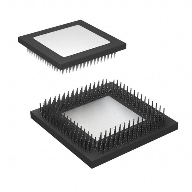
- Part No.:
- TMS320C80GF50
- Manufacturer:
- Texas Instruments
- Category:
- DSP (Digital Signal Processors)
- Package:
- 305-BFCPGA Exposed Pad
- Datasheet:
-
 TMS320C80GF50.pdf
- Description:
- IC MIMD DSP 305-CPGA
- Quantity:
- Payment:

- Shipping:

Inventory:1,712
Please send an inquiry. Send us your inquiry, and we will respond immediately.
Product details
Overview
TMS320C80GF50 from Texas Instruments is a single-chip parallel MIMD digital signal processor integrating a 32-bit RISC master processor with IEEE-754 floating-point capability, four 32-bit DSP parallel processors, a 480 MB/s transfer controller, and a dual-frame video controller. It delivers over two billion RISC-equivalent operations per second and features 50 KB of on-chip RAM, 3.3-V operation, and IEEE-1149.1 JTAG test access - optimized for real-time video encoding/decoding and high-speed imaging systems.
For engineers reviewing the TMS320C80GF50 datasheet, TMS320C80GF50 pinout, TMS320C80GF50 application, or TMS320C80GF50 equivalent, key selection considerations include its GF package (256-pin BGA), 16.6-ns cycle time, 4G-byte address space, DRAM/VRAM interface support, and dual independent video timing channels for simultaneous capture and display.
Technical Context
The TMS320C80GF50 implements a tightly coupled MIMD architecture with a shared on-chip crossbar enabling up to 15 concurrent memory accesses per cycle across the master processor, four parallel DSPs, and transfer controller. Each PP has dedicated 2 KB instruction cache and 8 KB data RAM, while the MP includes 4 KB instruction and 4 KB data caches.
Its transfer controller supports dynamic bus sizing, intelligent queuing, and direct DRAM/VRAM interfacing with 64-bit transfers at up to 480 MB/s. The video controller provides dual frame timers, composite/vertical blanking outputs, and programmable HSYNC/VSYNC I/O for synchronized dual-image systems.
Key Specifications
| Parameter | Value and Actual Design Meaning |
|---|---|
| Architecture | MIMD parallel processor with master RISC CPU + four 32-bit DSPs + TC + VC |
| Performance | Over 2 billion RISC-equivalent operations per second; 120 MFLOP IEEE-754 floating-point unit |
| On-Chip Memory | 50 KB RAM: 4 KB MP instruction cache, 4 KB MP data cache, 2 KB × 4 PP instruction caches, 8 KB × 4 PP data RAM |
| Transfer Rate | Up to 480 MB/s off-chip data transfer via 64-bit TC interface with dynamic bus sizing |
| Video Support | Dual independent frame timers; simultaneous capture/display; CBLNK/VBLNK, CSYNC/HBLNK, HSYNC/VSYNC I/O |
| Cycle Time | 16.6 ns (60 MHz operation); 3.3-V core and I/O supply |
| Address Space | 4 GB linear address space; lower 32 MB mapped to on-chip RAM and memory-mapped registers |
Pinout & Package
Package: GF package - 256-pin plastic ball grid array (BGA), bottom view, 1.27-mm pitch.
| Pin/Terminal | Circuit Role | Design Meaning |
|---|---|---|
| A5 | CT1 | Cycle-timing selection input; configures memory access timing parameters |
| A7, A9, A11, A13–A17, A19, A21, A23, A25, A27, A29, A31 | A0–A31 | 32-bit multiplexed address bus; supports DRAM row/column addressing and external memory mapping |
| D0–D63 | Data Bus | 64-bit bidirectional data path; enables high-bandwidth transfers between TC and external DRAM/VRAM |
| CAS/DQM0–CAS/DQM7 | Column Strobe / DQM | Eight byte-select strobes for DRAM/VRAM; provide byte-write capability and SDRAM DQM control |
| RAS | Row Address Strobe | Drives RAS inputs of DRAM/VRAM/SDRAM; initiates row-access cycles in conjunction with address bus |
| HSYNC0 / VSYNC0 | Video Timing I/O | Programmable horizontal/vertical sync pins for frame timer 0; support input synchronization or output generation |
Key Features
| Feature | Design Value |
|---|---|
| Single-chip MIMD architecture | Integrates MP, four PPs, TC, and VC on one die - eliminates inter-processor communication latency and board-level routing complexity |
| On-chip crossbar interconnect | Enables up to 15 concurrent memory accesses per cycle with round-robin arbitration - sustains peak throughput across all processing units |
| Dual independent video controllers | Supports simultaneous image capture and display using separate frame timers, blanking, and sync signals - enables real-time video pipelines |
| Dynamic DRAM/VRAM interface | BS0/BS1, PS0–PS3, CT0–CT2, UTIME enable automatic adaptation to diverse memory types, page sizes, and timing profiles |
| IEEE-1149.1 JTAG support | Full boundary-scan testability with TCK/TDI/TDO/TMS/TRST - enables production testing and in-system debug without additional probes |
Applications
| Video Surveillance Encoder | Medical Imaging Workstation |
|---|---|
Use Scenario: Real-time compression of multiple HD video streams from IP cameras into H.264 format for network transmission. IC Role / Device Role / Timing Role: TMS320C80GF50 acts as the primary video processing engine - its four parallel DSPs execute motion estimation, DCT, and quantization concurrently while the VC manages sensor frame capture timing. Use Value: Dual frame timers synchronize independent camera inputs; 480 MB/s TC bandwidth moves raw pixel data from VRAM to processing units without bottlenecking. |
Use Scenario: High-resolution ultrasound image reconstruction with real-time Doppler analysis and display overlay. IC Role / Device Role / Timing Role: TMS320C80GF50 serves as the real-time beamformer and post-processor - MP handles control flow while PPs execute FIR filtering and FFTs; VC drives dual-display output for live scan and processed image. Use Value: 50 KB on-chip RAM stores critical filter coefficients and intermediate buffers; 3.3-V operation ensures compatibility with low-noise analog front-end power domains. |
| Telecom Baseband Processor | Industrial Machine Vision Controller |
Use Scenario: Multi-carrier CDMA base station transceiver performing channel coding, modulation, and adaptive equalization. IC Role / Device Role / Timing Role: TMS320C80GF50 functions as the baseband signal processor - MP schedules tasks, PPs run Viterbi decoding and QAM demodulation, TC shuttles IQ samples to/from external ADC/DAC buffers. Use Value: 16.6-ns cycle time meets strict symbol-rate deadlines; IEEE-754 floating-point unit ensures numerical accuracy in adaptive algorithms. |
Use Scenario: PCB inspection system capturing and analyzing high-speed conveyor-belt images for defect detection using neural network inference kernels. IC Role / Device Role / Timing Role: TMS320C80GF50 operates as the embedded vision coprocessor - VC captures synchronized multi-camera frames; PPs execute convolution and thresholding; MP coordinates results reporting via host interface. Use Value: HREQ/HACK handshake allows seamless integration with host ARM controller; CAS/DQM strobes interface directly to high-density DDR SDRAM for frame buffering. |
Equivalent & Alternatives
The following parts are listed as comparable options for similar parallel DSP applications.
| Alternative Part | Technical Difference | Application Difference | Selection Advice |
|---|---|---|---|
| TMS320C82GHK | Same architecture but GHK package (272-pin PGA); lacks integrated video controller; lower TC bandwidth (320 MB/s) | Suitable for non-video DSP-intensive tasks like radar signal processing where video timing is irrelevant | Select when video subsystem is unnecessary and PGA socketing is preferred for prototyping |
| ADSP-TS201SABZ | 32-bit TigerSHARC DSP with 600 MHz core; no integrated TC or VC; uses external DMA controller; 256 KB L1 SRAM | Better suited for compute-dense FFT/filter banks without memory bandwidth constraints; requires external logic for DRAM/VRAM control | Choose for higher per-core throughput in non-video applications where external memory control is already implemented |
Compared with TMS320C80GF50, the TMS320C82GHK removes video functionality and reduces transfer bandwidth but offers PGA-based ease of replacement, while the ADSP-TS201SABZ trades integrated peripherals for higher clock rate and larger on-chip SRAM - making it preferable only when video timing and memory interface integration are not required.
Availability
TMS320C80GF50 is available at Aetrix Electronics and suitable for video surveillance encoders, medical imaging workstations, and telecom baseband processors requiring stable component supply and long-term industrial availability.
Supply support for TMS320C80GF50 includes scheduled delivery planning, volume procurement assistance, BOM continuity management, traceable sourcing, and lifecycle availability coordination for OEM customers, industrial embedded developers, connected-device designers, and electronics production programs.
Manufacturer
Texas Instruments is a global semiconductor leader specializing in analog, embedded processing, and digital signal processing technologies since 1930.
The TMS320C80 product line was designed specifically for high-throughput, real-time video and imaging systems requiring tightly integrated parallel processing, memory bandwidth, and video timing control - targeting broadcast, medical, and industrial vision markets.
FAQ
What is the package type and pin count of the TMS320C80GF50?
The TMS320C80GF50 uses the GF package: a 256-pin plastic ball grid array (BGA) with 1.27-mm pitch and bottom-view pinout. This package is distinct from the GGP variant (272-pin PGA) and is optimized for high-density PCB layouts in video processing modules. Pin assignments are fully documented in the SPRS023B datasheet, including dedicated video, memory, and JTAG terminals specific to the GF footprint.
Does the TMS320C80GF50 support both big-endian and little-endian operation?
Yes, the TMS320C80GF50 supports configurable endian mode. The UTIME pin determines endian selection during reset - if UTIME is high at the rising edge of RESET, the device boots in big-endian mode; if low, it initializes in little-endian mode. This setting affects data alignment in memory-mapped registers and instruction fetch behavior, and remains fixed until the next hardware reset.
How does the transfer controller (TC) interface with external DRAM or VRAM?
The TMS320C80GF50's transfer controller interfaces directly with DRAM/VRAM using dedicated control signals: RAS, CAS/DQM0–CAS/DQM7, TRG/CAS, W, DSF, and RL. It supports dynamic bus sizing via BS0/BS1, page-size configuration via PS0–PS3, and custom timing via CT0–CT2 and UTIME. The TC achieves up to 480 MB/s by issuing 64-bit transfers with intelligent queuing and cycle prioritization - eliminating need for external memory controllers.
Can the TMS320C80GF50 handle two independent video streams simultaneously?
Yes, the TMS320C80GF50 natively supports two independent video streams via its dual-frame video controller. Frame Timer 0 and Frame Timer 1 each drive separate HSYNC0/VSYNC0 and HSYNC1/VSYNC1 signals, with independent CBLNK/VBLNK and CSYNC/HBLNK configurations. This enables true simultaneous capture from one source and display to another - verified in reference designs for video conferencing and medical endoscopy systems.
What debugging and test capabilities does the TMS320C80GF50 provide?
The TMS320C80GF50 integrates full IEEE-1149.1 (JTAG) boundary-scan support via TCK, TDI, TDO, TMS, and TRST pins. It also includes EMU0/EMU1 emulation pins for multiprocessor halt-event signaling and host interrupt support. These features enable in-circuit debugging, structural testing, and real-time trace without requiring external emulators - critical for validating complex MIMD execution flows in the TMS320C80GF50.
TMS320C80GF50 Specifications
- Product attributes
- Attribute value
- Manufacturer:
- Texas Instruments
- Series:
- TMS320C8x
- Package/Case:
- 305-BFCPGA Exposed Pad
- Packaging:
- Tube
- Product Status:
- Obsolete
- Type:
- Floating Point
- Interface:
- Parallel
- Clock Rate:
- 50MHz
- Non-Volatile Memory:
- External
- On-Chip RAM:
- 98kB
- Voltage - I/O:
- 3.30V
- Voltage - Core:
- 3.30V
- Operating Temperature:
- 0°C ~ 85°C (TC)
- Grade:
- -
- Qualification:
- -
- Mounting Type:
- Through Hole
- Supplier Device Package:
- 305-CPGA (47.25x47.25)
TMS320C80GF50 FAQ
1.How can I place an order for TMS320C80GF50 through Aetrix?
Please submit a Request for Quotation (RFQ) for TMS320C80GF50 on Aetrix. Our sales agent will provide a competitive quotation and guide you through the order confirmation once you accept the terms.
2.Are the price and stock information for TMS320C80GF50 reliable?
The price and inventory of TMS320C80GF50 are updated periodically and may fluctuate due to market conditions. Stock and pricing data are typically refreshed every 24 hours. Quotation validity for TMS320C80GF50 is usually 5 days.
3.What payment methods are accepted for TMS320C80GF50?
We accept Wire Transfer, PayPal, Credit Card, Western Union, MoneyGram, and Escrow for TMS320C80GF50 transactions.
Note: Certain payment methods may incur a processing fee.
4.How is shipping managed for TMS320C80GF50?
TMS320C80GF50 orders can be shipped via leading logistics carriers, including DHL, UPS, FedEx, TNT, or Registered Mail.
Once your TMS320C80GF50 order is processed, you will receive an email with the shipment details and tracking number.
Note: Tracking information may take up to 24 hours to appear. Express delivery typically takes 3–5 business days.
5.How can I obtain technical support or documentation for TMS320C80GF50?
For technical support, including TMS320C80GF50 datasheets, pinout diagrams, or application guidance, please contact our engineering support team. They can provide detailed documentation and assistance for your TMS320C80GF50 requirements.
6.How does Aetrix verify that TMS320C80GF50 is sourced from the original manufacturer or authorized distributors?
All TMS320C80GF50 products on Aetrix are procured from qualified distributors and authorized channels. Our dedicated quality assurance team conducts strict verification, including traceability checks and, if necessary, third-party testing. This ensures that TMS320C80GF50 meets industry standards.
7.What is the process for return or replacement of TMS320C80GF50?
All TMS320C80GF50 units undergo pre-shipment inspection (PSI). If there is an issue with TMS320C80GF50, returns or replacements are accepted under the following conditions:
1.Quantity discrepancies, incorrect items, or visible external defects (such as breakage or corrosion), acknowledged by Aetrix.
2.The issue is reported within 90 days of delivery.
3.The TMS320C80GF50 part is unused and in its original packaging.
Return procedure for TMS320C80GF50:
1.Submit a request within 90 days.
2.Obtain a Return Material Authorization (RMA) from Aetrix.
TMS320C80GF50 Tags
-
TMS320C5535AZAY10
Texas Instruments
-
TMS320VC5501PGF300
Texas Instruments
-
ADSP-BF592KCPZ
Analog Devices Inc.
-
ADAU1463WBCPZ150
Analog Devices Inc.

-
TMS320VC5402PGE100
Texas Instruments

-
ADAU1701JSTZ-RL
Analog Devices Inc.
-
ADAU1701JSTZ
Analog Devices Inc.
-
TMS320VC5502PGF300
Texas Instruments
-
ADAU1462WBCPZ300RL
Analog Devices Inc.
-
ADAU1452KCPZRL
Analog Devices Inc.
-
ADAU1452WBCPZ-RL
Analog Devices Inc.
-
TMS320C6747DZKB3
Texas Instruments
Tech Hub

A practical engineering guide to 3.3V and 5V logic compatibility, input thresholds, resistor dividers, translator ICs, MOSFET level shifting, I2C pull-ups, timing limits and power-sequencing risks.

The 74HC595 uses push-pull logic outputs, while the TPIC6B595 uses 50 V open-drain DMOS sinks for higher-power loads. This guide compares timing, current limits, 3.3 V interfacing, load wiring, thermal…

The 74HC595 converts serial data into eight stable parallel outputs. This guide covers pin functions, shift and storage timing, OE and MR behavior, drive-current limits, cascading, voltage compatibilit…

A technical comparison of level-sensitive latches and edge-triggered flip-flops, covering timing windows, setup and hold limits, master–slave operation, time borrowing, race-through, HDL inference and…

A D latch stores one bit while Enable controls when data can pass. This reference covers gate-level operation, truth tables, transparency, setup and hold timing, LE versus OE, common ICs and practical …

An SR latch stores one bit through cross-coupled feedback. This engineering reference covers NOR and NAND implementations, truth tables, forbidden-state recovery, gated operation, switch debouncing, fa…

Latch circuits retain one bit through feedback. This technical reference covers SR and D latches, truth tables, transparency, timing limits, latch-versus-flip-flop behavior, applications and common log…

An engineering guide to LED driver operation, constant-current and constant-voltage outputs, linear and switching topologies, dimming, IC selection, calculations, replacement compatibility, and fault c…

Operational amplifier guide covering op amp basics, feedback, ideal vs real op amps, common configurations, buffer circuits, offset, bias current, gain-bandwidth, slew rate, rail-to-rail limits and sel…

Jumper cables guide covering safe connection order, red and black clamp placement, final ground connection, cable gauge, length, clamp quality, copper vs CCA cables, jump starter comparison and battery…


