
 My Inquiry
 My Account


Texas Instruments TMS3471C
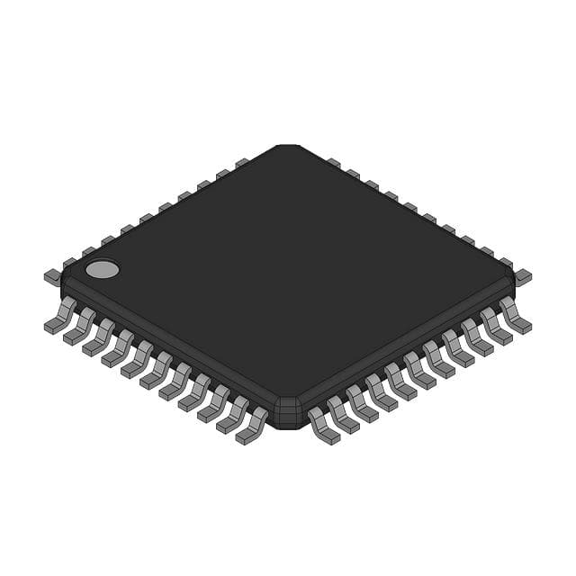
- Part No.:
- TMS3471C
- Manufacturer:
- Texas Instruments
- Category:
- Programmable Timers and Oscillators
- Package:
- -
- Datasheet:
-
 TMS3471C.pdf
- Description:
- CONSUMER CIRCUIT, PQFP44
- Quantity:
- Payment:

- Shipping:

Inventory:700
Please send an inquiry. Send us your inquiry, and we will respond immediately.
Product details
Overview
TMS3471C from Texas Instruments is a monolithic NTSC timing generator IC designed specifically to drive the TI TC241 monochrome CCD image sensor. It delivers synchronized CCD drive signals (PI, PS, T, GT1–3), NTSC sync outputs (CSYNC, CBLK, BF, SC, SC(90)), and sample-and-hold pulses (SH1, SH2,3) using a single 5-V supply and 14.318-MHz crystal input. It operates from –20°C to 45°C in a 44-pin plastic flat package.
For engineers reviewing the TMS3471C datasheet, TMS3471C pinout, TMS3471C application, or TMS3471C equivalent, key selection considerations include NTSC-compatible timing accuracy, eight selectable antiblooming modes, clamp-pulse configuration options, vertical/horizontal counter synchronization, and compatibility with TI's TMS3472A/TMS3473B drivers and TL1593/TL1051 video signal processors.
Technical Context
The TMS3471C integrates a 14.318-MHz crystal oscillator, divide-by-4 and divide-by-7 logic to generate 3.58-MHz subcarrier and 2.045-MHz vertical timing, respectively. Its horizontal and vertical counters produce precisely timed gate clocks (HGATE, VGATE), transfer pulses (T), and storage/parallel-area clocks (PS, PI) aligned to NTSC 525-line/60-Hz frame structure.
It implements configurable antiblooming via ABS0–ABS2 inputs selecting among eight clocking modes (250 kHz–2.2 MHz, flyback-only or continuous), while BCPS0/BCPS1 control optical black clamp pulse placement relative to horizontal scan. E/L selects early/late serial-transfer timing versus sample-and-hold, and VDS sets vertical-dump frequency (1 MHz or 2 MHz) or functions as a reset input.
Key Specifications
| Parameter | Value and Actual Design Meaning |
|---|---|
| Supply Voltage | 4.5 V to 5.5 V - ensures stable operation with standard TTL/CMOS logic rails and low-noise analog timing paths. |
| Input Clock Frequency | 14.31818 MHz - matches NTSC color burst standard for precise subcarrier and line-rate derivation. |
| Operating Temperature | –20°C to 45°C - qualified for industrial and commercial imaging equipment environments. |
| Average Supply Current | 40 mA at VCC = 5 V - defines power budget for CCD camera timing subsystems. |
| Output Drive Strength | ±1 mA on BCP1/BCP2; ±0.3–0.6 mA on SC/SC(90)/CP2 - sufficient to drive capacitive loads up to 50 pF without external buffering. |
| Timing Skew | ±5 ns between S1/S2,3 and GT1/GT2 rising/falling edges - enables tight inter-clock alignment critical for CCD charge transfer fidelity. |
| Antiblooming Modes | 8 discrete configurations via ABS0–ABS2 - allows optimization of blooming suppression vs. power consumption across lighting conditions. |
Pinout & Package
Package: FS/S-PQFP-G44 - 44-pin plastic quad flatpack with 0.55 mm max lead pitch, 17.40–18.20 mm body length, and 14.20 mm max square footprint.
| Pin/Terminal | Circuit Role | Design Meaning |
|---|---|---|
| GND (33) | Ground reference | Common return for all analog and digital circuitry; must be low-impedance for timing stability. |
| VCC (22) | Power supply | Single 5-V DC input powering internal oscillators, counters, and output drivers. |
| X1 (34), X2 (35) | Crystal oscillator interface | Direct connection point for 14.318-MHz fundamental-mode crystal; internal oscillator circuitry requires no external buffer. |
| ABIN (29) | Antiblooming output | Drives ABG input of TC240/TC241 CCD sensors to suppress charge overflow during integration. |
| PS (27), PI (30), T (23) | CCD gate clocks | Generate parallel-storage, parallel-image, and transfer-gate timing waveforms synchronized to NTSC horizontal scan. |
| GT1 (36), GT2 (37), GT3 (38) | Y-gate outputs | Provide decoded vertical timing for CCD row selection; used with TI TMS3473B parallel driver. |
| SH1 (32), SH2,3 (31) | Sample-and-hold control | Trigger TI TL1593 three-channel S/H for correlated double sampling of CCD video output. |
| BCP1 (44), BCP2 (1) | Optical black clamp pulses | Enable black-level calibration by clamping CCD output during optical black intervals; placement controlled by BCPS0/BCPS1. |
| CSYNC (4), CBLK (5), BF (6) | NTSC sync signals | Provide composite sync, composite blank, and burst flag for video processor synchronization per NTSC RS-170 standard. |
| SC (7), SC(90) (8) | Subcarrier outputs | Deliver 3.58-MHz color subcarrier and its 90° phase-shifted version for chroma demodulation circuits. |
Key Features
| Feature | Design Value |
|---|---|
| NTSC-timing operation | Generates fully compliant 525-line/60-Hz timing including CSYNC, CBLK, BF, and 3.58-MHz SC - eliminates need for external sync generators in monochrome CCTV cameras. |
| Eight selectable antiblooming modes | Configurable via ABS0–ABS2 to match sensor illumination conditions - prevents white saturation in high-contrast scenes without firmware changes. |
| Clamp-pulse select option | BCPS0/BCPS1 inputs adjust BCP1/BCP2 timing relative to horizontal scan - enables precise black-level calibration across varying pixel clock rates. |
| Delayed horizontal transfer | E/L input shifts S1/S2,3 serial-transfer pulses early or late versus SH1/SH2,3 - supports flexible readout sequencing for different CCD architectures. |
| Vertical-dump speed control | VDS input selects 1 MHz or 2 MHz vertical dump rate - adapts frame rate handling for interlaced vs. progressive scan modes or fast-clear operations. |
Applications
| Monochrome CCTV Camera | Industrial Machine Vision Sensor |
|---|---|
Use Scenario: Fixed-mount surveillance camera capturing 2/3-inch monochrome CCD output under variable lighting. IC Role / Device Role / Timing Role: Primary NTSC timing generator providing PI/PS/T gate clocks, SH1/SH2,3 sample pulses, and CSYNC/CBLK/SC for video encoder interface. Use Value: Eliminates discrete timing logic and crystal oscillators, reducing BOM count and layout area while ensuring broadcast-compliant sync timing. | Use Scenario: Factory-floor inspection system requiring repeatable black-level calibration and antiblooming control for defect detection. IC Role / Device Role / Timing Role: CCD timing controller delivering configurable BCP1/BCP2 clamp pulses, eight antiblooming modes, and precise GT1–GT3 Y-gate sequencing. Use Value: Enables dynamic adjustment of blooming suppression and optical black timing without hardware change - improves yield in high-contrast production environments. |
| Medical Endoscope Imaging Module | Legacy Broadcast Equipment Repair |
Use Scenario: Compact endoscopic camera using TI TC241 CCD sensor needing low-power, reliable timing in constrained thermal envelope. IC Role / Device Role / Timing Role: Integrated timing solution supplying 5-V powered NTSC sync, sample-and-hold triggers, and power-down (PD) mode for energy management. Use Value: Reduces standby current to 15 mA and supports rapid power cycling via SB input - extends battery life in portable diagnostic tools. | Use Scenario: Restoration of vintage NTSC video test equipment requiring authentic timing signal generation for waveform verification. IC Role / Device Role / Timing Role: Drop-in replacement for original TMS3471C-based timing boards, reproducing exact CSYNC, CBLK, BF, SC, and SC(90) phasing. Use Value: Maintains legacy signal integrity and timing relationships defined in SOCS028B datasheet - avoids redesign of analog video path compensation networks. |
Equivalent & Alternatives
The following parts are listed as comparable options for similar NTSC timing generator applications.
| Alternative Part | Technical Difference | Application Difference | Selection Advice |
|---|---|---|---|
| TMS3471 | Same functionality but characterized for 0°C to 70°C; lacks explicit –20°C low-temp qualification. | Suitable for commercial indoor systems; not rated for cold-environment CCTV enclosures. | Select TMS3471 only if ambient operating temperature remains ≥0°C. |
| TMS3471A | Revised version with improved ESD tolerance (4 kV HBM vs. 2 kV); identical timing specs and pinout. | Preferred for new designs requiring higher robustness against handling ESD in manufacturing. | Choose TMS3471A when board-level ESD immunity is critical and legacy TMS3471C footprint compatibility is required. |
Compared with TMS3471C, TMS3471 offers wider temperature margin above zero but no cold-start capability, while TMS3471A provides enhanced ESD protection without altering timing behavior - making it the recommended upgrade path for reliability-critical deployments where the –20°C lower limit is not mandatory.
Availability
TMS3471C is available at Aetrix Electronics and suitable for monochrome CCTV cameras, industrial machine vision sensors, medical endoscope modules, and legacy broadcast equipment repair requiring stable component supply and long-lifecycle support.
Supply support for TMS3471C includes scheduled delivery planning, volume procurement assistance, BOM continuity management, traceable sourcing, and lifecycle availability coordination for OEM customers, industrial embedded developers, connected-device designers, and electronics production programs.
Manufacturer
Texas Instruments is a global semiconductor company founded in 1930, specializing in analog, embedded processing, and digital signal technologies with broad industrial and automotive reach.
The TMS3471C belongs to TI's legacy imaging timing product line, engineered specifically to support 2/3-inch monochrome CCD sensors like the TC241 in NTSC-standard video acquisition systems.
FAQ
What is the primary function of the TMS3471C in a CCD imaging system?
The TMS3471C serves as the core NTSC timing generator for 2/3-inch monochrome CCD sensors such as the TI TC241. It produces all essential drive signals - including parallel-storage (PS), parallel-image (PI), and transfer-gate (T) clocks - along with NTSC synchronization outputs (CSYNC, CBLK, BF, SC, SC(90)) and sample-and-hold pulses (SH1, SH2,3). Its design eliminates the need for discrete timing logic in broadcast-compliant monochrome video systems.
Does the TMS3471C support both interlaced and noninterlaced scanning modes?
Yes, the TMS3471C supports both interlaced and noninterlaced operation via the I/N (interlace select) input. When I/N is high, the device generates timing for interlaced NTSC fields (262.5 lines per field); when low, it configures for noninterlaced (progressive) scanning. This flexibility allows use in both traditional CCTV and specialized machine vision applications requiring full-frame capture.
How does the TMS3471C implement antiblooming control, and what are the configuration options?
The TMS3471C implements antiblooming through the ABIN output and three digital inputs - ABS0, ABS1, and ABS2 - which select among eight distinct antiblooming modes. These modes define whether antiblooming pulses occur continuously or only during vertical flyback, and at frequencies of 250 kHz, 500 kHz, 1 MHz, or 2.2 MHz. The configuration is static and set at power-on, enabling optimization for specific lighting and scene-dynamic-range requirements.
Can the TMS3471C operate with a 5-V supply only, or does it require additional voltage rails?
The TMS3471C operates exclusively from a single 5-V supply (VCC = 4.5 V to 5.5 V), with no auxiliary voltage rails required. All internal circuitry - including the crystal oscillator, counters, logic, and output drivers - is designed for 5-V CMOS/TTL compatibility. Ground (GND) is the sole reference, and unused inputs must be tied to VCC or GND to prevent floating states that could increase power consumption or cause erratic timing.
What is the role of the VDS pin on the TMS3471C, and how does it affect vertical timing?
The VDS pin on the TMS3471C controls vertical-dump speed: when high, it selects a 2.045-MHz vertical-dump frequency; when low, it selects 1.022-MHz. Additionally, VDS can serve as a hardware reset input - dropping its voltage from VCC to VCC/2 and back triggers a timer reset. This dual function enables both frame-rate adaptation and safe recovery from timing lock-up without requiring external logic.
TMS3471C Specifications
- Product attributes
- Attribute value
- Manufacturer:
- Texas Instruments
- Series:
- *
- Package/Case:
- -
- Packaging:
- Bulk
- Product Status:
- Active
- Type:
- -
- Count:
- -
- Frequency:
- -
- Voltage - Supply:
- -
- Current - Supply:
- -
- Operating Temperature:
- -
- Supplier Device Package:
- -
- Mounting Type:
- -
- Grade:
- -
- Qualification:
- -
TMS3471C FAQ
1.How can I place an order for TMS3471C through Aetrix?
Please submit a Request for Quotation (RFQ) for TMS3471C on Aetrix. Our sales agent will provide a competitive quotation and guide you through the order confirmation once you accept the terms.
2.Are the price and stock information for TMS3471C reliable?
The price and inventory of TMS3471C are updated periodically and may fluctuate due to market conditions. Stock and pricing data are typically refreshed every 24 hours. Quotation validity for TMS3471C is usually 5 days.
3.What payment methods are accepted for TMS3471C?
We accept Wire Transfer, PayPal, Credit Card, Western Union, MoneyGram, and Escrow for TMS3471C transactions.
Note: Certain payment methods may incur a processing fee.
4.How is shipping managed for TMS3471C?
TMS3471C orders can be shipped via leading logistics carriers, including DHL, UPS, FedEx, TNT, or Registered Mail.
Once your TMS3471C order is processed, you will receive an email with the shipment details and tracking number.
Note: Tracking information may take up to 24 hours to appear. Express delivery typically takes 3–5 business days.
5.How can I obtain technical support or documentation for TMS3471C?
For technical support, including TMS3471C datasheets, pinout diagrams, or application guidance, please contact our engineering support team. They can provide detailed documentation and assistance for your TMS3471C requirements.
6.How does Aetrix verify that TMS3471C is sourced from the original manufacturer or authorized distributors?
All TMS3471C products on Aetrix are procured from qualified distributors and authorized channels. Our dedicated quality assurance team conducts strict verification, including traceability checks and, if necessary, third-party testing. This ensures that TMS3471C meets industry standards.
7.What is the process for return or replacement of TMS3471C?
All TMS3471C units undergo pre-shipment inspection (PSI). If there is an issue with TMS3471C, returns or replacements are accepted under the following conditions:
1.Quantity discrepancies, incorrect items, or visible external defects (such as breakage or corrosion), acknowledged by Aetrix.
2.The issue is reported within 90 days of delivery.
3.The TMS3471C part is unused and in its original packaging.
Return procedure for TMS3471C:
1.Submit a request within 90 days.
2.Obtain a Return Material Authorization (RMA) from Aetrix.
TMS3471C Tags

-
NE555DR
Texas Instruments
-
SA555DR
Texas Instruments
-
NA555DR
Texas Instruments
-
SE555DR
Texas Instruments

-
NE555P
Texas Instruments

-
CD4541BM96
Texas Instruments

-
CD4541BE
Texas Instruments
-
TLC555QDR
Texas Instruments
-
TLC555IDR
Texas Instruments
-
TLC555QDRQ1
Texas Instruments

-
TPL5010DDCR
Texas Instruments
-
TLC555CP
Texas Instruments
Tech Hub

A practical engineering guide to 3.3V and 5V logic compatibility, input thresholds, resistor dividers, translator ICs, MOSFET level shifting, I2C pull-ups, timing limits and power-sequencing risks.

The 74HC595 uses push-pull logic outputs, while the TPIC6B595 uses 50 V open-drain DMOS sinks for higher-power loads. This guide compares timing, current limits, 3.3 V interfacing, load wiring, thermal…

The 74HC595 converts serial data into eight stable parallel outputs. This guide covers pin functions, shift and storage timing, OE and MR behavior, drive-current limits, cascading, voltage compatibilit…

A technical comparison of level-sensitive latches and edge-triggered flip-flops, covering timing windows, setup and hold limits, master–slave operation, time borrowing, race-through, HDL inference and…

A D latch stores one bit while Enable controls when data can pass. This reference covers gate-level operation, truth tables, transparency, setup and hold timing, LE versus OE, common ICs and practical …

An SR latch stores one bit through cross-coupled feedback. This engineering reference covers NOR and NAND implementations, truth tables, forbidden-state recovery, gated operation, switch debouncing, fa…

Latch circuits retain one bit through feedback. This technical reference covers SR and D latches, truth tables, transparency, timing limits, latch-versus-flip-flop behavior, applications and common log…

An engineering guide to LED driver operation, constant-current and constant-voltage outputs, linear and switching topologies, dimming, IC selection, calculations, replacement compatibility, and fault c…

Operational amplifier guide covering op amp basics, feedback, ideal vs real op amps, common configurations, buffer circuits, offset, bias current, gain-bandwidth, slew rate, rail-to-rail limits and sel…

Jumper cables guide covering safe connection order, red and black clamp placement, final ground connection, cable gauge, length, clamp quality, copper vs CCA cables, jump starter comparison and battery…


