
 My Inquiry
 My Account


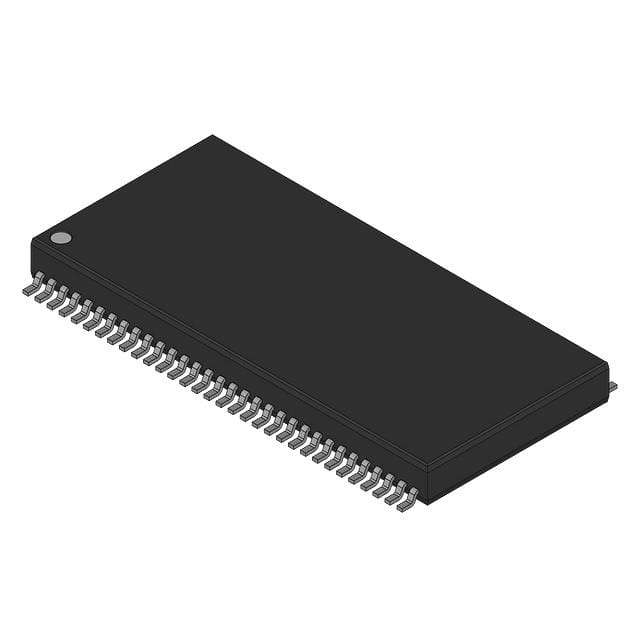
Texas Instruments TMS55165-70ADGH
- Part No.:
- TMS55165-70ADGH
- Manufacturer:
- Texas Instruments
- Category:
- Memory
- Package:
- -
- Datasheet:
-
 TMS55165-70ADGH.pdf
- Description:
- VIDEO DRAM, 256KX16, 70NS PDSO64
- Quantity:
- Payment:

- Shipping:

Inventory:240
Please send an inquiry. Send us your inquiry, and we will respond immediately.
Product details
Overview
TMS55165-70ADGH from Texas Instruments is a 262,144 × 16-bit dual-port video RAM with DRAM + serial-access memory (SAM) architecture, supporting simultaneous asynchronous access to both ports, 4-column block-write, write-per-bit masking, and enhanced page mode - deployed in high-bandwidth CRT-based graphics controllers and video frame buffers.
For engineers reviewing the TMS55165-70ADGH datasheet, TMS55165-70ADGH pinout, TMS55165-70ADGH application, or TMS55165-70ADGH equivalent, key selection considerations include its 70 ns DRAM row-access time, 20 ns serial-data access minimum, 40 ns DRAM page-cycle time, 5.0 V ± 0.5 V supply, and DGH 64-pin SOIC package compatibility with TI's legacy graphics ecosystem.
Technical Context
The TMS55165-70ADGH integrates a 262,144-word × 16-bit DRAM array with a 256-word × 16-bit static serial-access memory (SAM), enabling real-time pixel streaming via 55 MHz uninterrupted serial output. Its dual-port architecture allows concurrent DRAM random access and SAM serial readout without arbitration overhead.
It implements CAS-before-RAS (CBR) and hidden refresh for 8 ms maximum refresh interval, supports full-register and split-register transfer modes between DRAM and SAM, and uses on-chip address latching with TTL-compatible I/Os - all fabricated in TI's EPIC CMOS process for stability in embedded video systems.
Key Specifications
| Parameter | Value and Actual Design Meaning |
|---|---|
| Memory Organization | 262,144 words × 16 bits DRAM + 256 words × 16 bits serial-access memory (SAM) |
| Access Time (tRAC) | 70 ns max - defines worst-case latency from RAS fall to valid DRAM data output |
| Serial Access Time (tSCA) | 20 ns min - sets minimum SC-to-SQ propagation delay for high-speed pixel clocking |
| DRAM Page Cycle (tPC) | 40 ns min - enables rapid sequential column reads within same row for scanline rendering |
| Supply Voltage | 5.0 V ± 0.5 V - requires tightly regulated single-rail supply; no voltage translation needed for TTL logic |
| Block-Write Capability | 4-column only - writes 16-bit color data to four adjacent columns per CAS cycle, up to 64 bits total |
| Refresh Interval | 8 ms max - reduces system-level refresh overhead vs. standard 2 ms DRAMs |
Pinout & Package
Package: 64-pin small-outline gull-wing-leaded (DGH), surface-mount, JEDEC MS-026 compliant. All VCC and VSS pins must be individually decoupled; NC/GND pins are unconnected internally and may be tied to ground externally.
| Pin/Terminal | Circuit Role | Design Meaning |
|---|---|---|
| A0–A8 | Address Inputs | Latched on RAS/CAS fall for row/column/block addressing; A0–A1 ignored in 4-column block-write |
| RAS | Row-Address Strobe | Initiates row access, latches row address and control signals; also acts as DRAM output enable |
| CAS | Column-Address Strobe | Latches column/block/tap address; functions as DRAM output enable and SAM tap-address strobe |
| WEL / WEU | Write Enable / Byte Select | WEL controls DQ0–DQ7 write; WEU controls DQ8–DQ15 write; both low enables write-per-bit mask loading |
| DQ0–DQ15 | DRAM Data I/O | Bidirectional 16-bit bus; latched on CAS or WEx fall; carries data, write mask, or column mask depending on mode |
| SQ0–SQ15 | Serial Data Output | 3-state TTL-compatible outputs; driven on SC rising edge; enabled by SE low |
| SC / SE | Serial Clock / Serial Enable | SC increments SAM address counter; SE enables SQ/QSF outputs but does not gate SC operation |
| TRG | Transfer Select / Output Enable | High on RAS fall selects DRAM access; low selects DRAM→SAM transfer; also enables DRAM outputs |
| DSF | Special Function Select | Latched on RAS/CAS fall to configure block-write, load-mask-register, or load-color-register cycles |
| QSF | Serial Register Status | Indicates active SAM half: low = lower 128 bits, high = upper 128 bits - critical for split-register timing |
Key Features
| Feature | Design Value |
|---|---|
| Split-Register Transfer | Enables real-time serial streaming: one SAM half outputs while the other loads from DRAM - eliminates blanking-period dependency |
| 4-Column Block-Write | Writes 16-bit color value to four adjacent column addresses per CAS cycle, accelerating area-fill and line-draw operations |
| Persistent Write-Per-Bit | Mask register retains write-enable state across multiple cycles after LMR command - reduces bus bandwidth for partial writes |
| Enhanced Page Mode | Allows column address setup before CAS fall, reducing effective access time for sequential pixel reads within a scanline |
| CBR & Hidden Refresh | Internal row addressing during CBR or CAS-held refresh eliminates external address generation and preserves DRAM output validity |
Applications
| Video Frame Buffer | Graphics Controller Interface |
|---|---|
Use Scenario: Stores full-resolution raster frames for CRT display output at 60 Hz interlaced or progressive scan. IC Role / Device Role / Timing Role: Dual-port memory serving as pixel store: DRAM port accepts CPU/GPU updates; SAM port streams pixels synchronously to video DAC. Use Value: 55 MHz serial stream supports ≥1024×768 @ 60 Hz with 16-bit color depth; split-register transfer enables continuous output during active display period. |
Use Scenario: Embedded in TI TMS340x0 graphics processors for local display list and attribute storage. IC Role / Device Role / Timing Role: Co-processor memory mapped to graphics engine's DRAM port; SAM port feeds pixel pipeline under SC-controlled timing. Use Value: 4-column block-write accelerates polygon fill and line drawing; byte-write enables efficient palette and attribute updates without full-word writes. |
| Industrial Video Overlay | Legacy Broadcast Equipment |
Use Scenario: Real-time overlay of text or graphics onto live analog video feed using genlock-synchronized sampling. IC Role / Device Role / Timing Role: DRAM port receives overlay bitmap from host processor; SAM port outputs pixel-aligned overlay stream synchronized to horizontal sync. Use Value: QSF pin provides half-register status for precise timing alignment; 3-state SQ outputs allow multiplexing with baseband video signal. |
Use Scenario: Character generator and font buffer in broadcast character inserter units (e.g., Telestream, FOR-A). IC Role / Device Role / Timing Role: Stores ASCII glyph bitmaps in DRAM; SAM port serially clocks out 16-bit pixel rows to video shift register at dot-clock rate. Use Value: Full-register transfer preloads entire glyph row into SAM; enhanced page mode enables fast glyph fetch during horizontal retrace. |
Equivalent & Alternatives
The following parts are listed as comparable options for similar dual-port video RAM applications.
| Alternative Part | Technical Difference | Application Difference | Selection Advice |
|---|---|---|---|
| TMS55166-70ADGH | Same 4-column block-write and package, but adds Extended Data Output (EDO) mode - DRAM output remains valid after CAS high | Enables tighter system timing in EDO-capable controllers; requires compatible controller support for EDO handshake | Select TMS55166-70ADGH only if host controller implements EDO protocol; otherwise TMS55165-70ADGH ensures full backward compatibility |
| TMS55175-70ADGH | Same speed grade and package, but supports 8-column block-write (vs. 4-column) - doubles per-CAS block data throughput | Optimized for higher pixel density displays or faster area-fill; requires updated address mapping for block addressing (A3–A8 used) | Choose TMS55175-70ADGH when application demands >64-bit per-CAS block writes; verify address decoder logic supports A3–A8 block addressing |
Compared with TMS55166-70ADGH and TMS55175-70ADGH, the TMS55165-70ADGH offers strict page-mode timing compliance and minimal interface complexity - ideal for legacy TI graphics designs where EDO or 8-column block-write features are unused or unsupported.
Availability
TMS55165-70ADGH is available at Aetrix Electronics and suitable for industrial video frame buffers, CRT-based graphics controllers, broadcast character generators, and legacy embedded display subsystems requiring stable component supply and long-term obsolescence management.
Supply support for TMS55165-70ADGH includes scheduled delivery planning, volume procurement assistance, BOM continuity management, traceable sourcing, and lifecycle availability coordination for OEM customers, industrial embedded developers, connected-device designers, and electronics production programs.
Manufacturer
Texas Instruments is a U.S.-based semiconductor company founded in 1930, specializing in analog, embedded processing, and digital signal technologies with broad industrial and automotive reach.
The TMS551xx family was designed specifically for high-bandwidth video memory applications in 1990s-era graphics systems - integrating DRAM density with serial-access performance to offload pixel streaming from main processors.
FAQ
What is the maximum serial data rate supported by the TMS55165-70ADGH?
The TMS55165-70ADGH supports uninterrupted serial-data streams up to 55 MHz, corresponding to a minimum serial cycle time (tSCC) of 22 ns. This enables real-time pixel output for resolutions such as 1024×768 at 60 Hz with 16-bit color depth, provided the external SC clock meets setup/hold timing relative to SE and QSF.
Does the TMS55165-70ADGH support extended data output (EDO) mode?
No, the TMS55165-70ADGH does not support EDO mode. EDO functionality is exclusive to the TMS551x6 series (e.g., TMS55166). The TMS55165-70ADGH operates in standard page-mode DRAM timing, where DRAM output is invalidated when CAS returns high - confirmed in Table 1 and functional description sections of the SMVS463 datasheet.
How is the 4-column block-write function configured on the TMS55165-70ADGH?
The 4-column block-write function is activated by asserting DSF high on RAS fall and high on CAS fall, with WEL/WEU set appropriately. Column address bits A2–A8 define the block address selecting one of 128 blocks per row; A0–A1 are ignored. Each block-write cycle transfers 16 bits of color data to four adjacent columns, up to 64 bits per CAS cycle.
Can the TMS55165-70ADGH perform simultaneous DRAM and SAM access without conflict?
Yes, the TMS55165-70ADGH supports true simultaneous and asynchronous access to both ports except during DRAM→SAM transfer operations. The DRAM port handles CPU/GPU writes or reads while the SAM port streams serial pixel data - enabled by independent address/control paths and separate output buffers verified in the functional block diagram and timing tables.
What is the purpose of the QSF pin on the TMS55165-70ADGH?
The QSF (Serial Register Status) pin indicates which half of the 256-word SAM is currently active: QSF = low for the lower 128 bits (addresses 0–127), QSF = high for the upper 128 bits (addresses 128–255). It is essential for synchronizing external logic during split-register-transfer operations and aligning serial output with display timing requirements.
TMS55165-70ADGH Specifications
- Product attributes
- Attribute value
- Manufacturer:
- Texas Instruments
- Series:
- *
- Package/Case:
- -
- Packaging:
- Bulk
- Product Status:
- Active
- Programmable:
- Not Verified
- Memory Type:
- -
- Memory Format:
- -
- Technology:
- -
- Memory Size:
- -
- Memory Organization:
- -
- Memory Interface:
- -
- Clock Frequency:
- -
- Write Cycle Time - Word, Page:
- -
- Access Time:
- -
- Voltage - Supply:
- -
- Operating Temperature:
- -
- Grade:
- -
- Qualification:
- -
- Mounting Type:
- -
- Supplier Device Package:
- -
TMS55165-70ADGH FAQ
1.How can I place an order for TMS55165-70ADGH through Aetrix?
Please submit a Request for Quotation (RFQ) for TMS55165-70ADGH on Aetrix. Our sales agent will provide a competitive quotation and guide you through the order confirmation once you accept the terms.
2.Are the price and stock information for TMS55165-70ADGH reliable?
The price and inventory of TMS55165-70ADGH are updated periodically and may fluctuate due to market conditions. Stock and pricing data are typically refreshed every 24 hours. Quotation validity for TMS55165-70ADGH is usually 5 days.
3.What payment methods are accepted for TMS55165-70ADGH?
We accept Wire Transfer, PayPal, Credit Card, Western Union, MoneyGram, and Escrow for TMS55165-70ADGH transactions.
Note: Certain payment methods may incur a processing fee.
4.How is shipping managed for TMS55165-70ADGH?
TMS55165-70ADGH orders can be shipped via leading logistics carriers, including DHL, UPS, FedEx, TNT, or Registered Mail.
Once your TMS55165-70ADGH order is processed, you will receive an email with the shipment details and tracking number.
Note: Tracking information may take up to 24 hours to appear. Express delivery typically takes 3–5 business days.
5.How can I obtain technical support or documentation for TMS55165-70ADGH?
For technical support, including TMS55165-70ADGH datasheets, pinout diagrams, or application guidance, please contact our engineering support team. They can provide detailed documentation and assistance for your TMS55165-70ADGH requirements.
6.How does Aetrix verify that TMS55165-70ADGH is sourced from the original manufacturer or authorized distributors?
All TMS55165-70ADGH products on Aetrix are procured from qualified distributors and authorized channels. Our dedicated quality assurance team conducts strict verification, including traceability checks and, if necessary, third-party testing. This ensures that TMS55165-70ADGH meets industry standards.
7.What is the process for return or replacement of TMS55165-70ADGH?
All TMS55165-70ADGH units undergo pre-shipment inspection (PSI). If there is an issue with TMS55165-70ADGH, returns or replacements are accepted under the following conditions:
1.Quantity discrepancies, incorrect items, or visible external defects (such as breakage or corrosion), acknowledged by Aetrix.
2.The issue is reported within 90 days of delivery.
3.The TMS55165-70ADGH part is unused and in its original packaging.
Return procedure for TMS55165-70ADGH:
1.Submit a request within 90 days.
2.Obtain a Return Material Authorization (RMA) from Aetrix.
TMS55165-70ADGH Tags

-
M24C02-WMN6TP
STMicroelectronics

-
AT24C02C-XHM-T
Microchip Technology

-
AT21CS01-STUM10-T
Microchip Technology

-
AT24C02C-SSHM-T
Microchip Technology

-
24LC01BT-I/OT
Microchip Technology

-
M24C02-FMC6TG
STMicroelectronics
-
AT24CS02-SSHM-T
Microchip Technology

-
93LC46BT-I/OT
Microchip Technology
-
AT24C04C-SSHM-T
Microchip Technology

-
24LC01BT-I/SN
Microchip Technology
-
24AA02UIDT-I/OT
Microchip Technology

-
AT24C08C-STUM-T
Microchip Technology
Tech Hub

A practical engineering guide to 3.3V and 5V logic compatibility, input thresholds, resistor dividers, translator ICs, MOSFET level shifting, I2C pull-ups, timing limits and power-sequencing risks.

The 74HC595 uses push-pull logic outputs, while the TPIC6B595 uses 50 V open-drain DMOS sinks for higher-power loads. This guide compares timing, current limits, 3.3 V interfacing, load wiring, thermal…

The 74HC595 converts serial data into eight stable parallel outputs. This guide covers pin functions, shift and storage timing, OE and MR behavior, drive-current limits, cascading, voltage compatibilit…

A technical comparison of level-sensitive latches and edge-triggered flip-flops, covering timing windows, setup and hold limits, master–slave operation, time borrowing, race-through, HDL inference and…

A D latch stores one bit while Enable controls when data can pass. This reference covers gate-level operation, truth tables, transparency, setup and hold timing, LE versus OE, common ICs and practical …

An SR latch stores one bit through cross-coupled feedback. This engineering reference covers NOR and NAND implementations, truth tables, forbidden-state recovery, gated operation, switch debouncing, fa…

Latch circuits retain one bit through feedback. This technical reference covers SR and D latches, truth tables, transparency, timing limits, latch-versus-flip-flop behavior, applications and common log…

An engineering guide to LED driver operation, constant-current and constant-voltage outputs, linear and switching topologies, dimming, IC selection, calculations, replacement compatibility, and fault c…

Operational amplifier guide covering op amp basics, feedback, ideal vs real op amps, common configurations, buffer circuits, offset, bias current, gain-bandwidth, slew rate, rail-to-rail limits and sel…

Jumper cables guide covering safe connection order, red and black clamp placement, final ground connection, cable gauge, length, clamp quality, copper vs CCA cables, jump starter comparison and battery…


