
 My Inquiry
 My Account


Texas Instruments TP13054BDWR
- Part No.:
- TP13054BDWR
- Manufacturer:
- Texas Instruments
- Category:
- CODECS
- Package:
- -
- Datasheet:
-
 TP13054BDWR.pdf
- Description:
- PCM CODEC, MU-LAW, 1-FUNC, CMOS
- Quantity:
- Payment:

- Shipping:

Inventory:14,895
Please send an inquiry. Send us your inquiry, and we will respond immediately.
Product details
Overview
TP13054BDWR from Texas Instruments is a monolithic PCM codec and filter IC designed for full-duplex voice telephony interface in TDM systems. It integrates µ-law A/D and D/A conversion, transmit high-pass/low-pass filtering, receive low-pass filtering with (sin x)/x correction, active RC noise filters, and internal precision voltage reference. Operates at ±5 V, delivers 50 mW typical active power, supports –40°C to 85°C industrial temperature range, and targets line interface cards in T1/PABX/central office systems.
For engineers reviewing the TP13054BDWR datasheet, TP13054BDWR pinout, TP13054BDWR application, or TP13054BDWR equivalent, key selection criteria include µ-law PCM compatibility, dual master clock support (1.536/1.544/2.048 MHz), short- or long-frame sync flexibility, transmit idle noise performance (≤9 dBrnC₀), and industrial-grade thermal specification.
Technical Context
The TP13054BDWR implements a complete analog-to-digital and digital-to-analog signal chain for voice-band PCM systems, with integrated switched-capacitor band-pass and low-pass filters on transmit and receive paths. Its architecture includes autozero circuitry for offset stability, TTL/CMOS-compatible serial I/O, and independent transmit/receive frame-sync and bit-clock domains.
It supports both synchronous (MCLKX only, MCLKR/PDN as power-down control) and asynchronous (separate MCLKX/MCLKR) operation modes, with automatic 193rd-pulse compensation for 1.544 MHz T1 framing. The device uses internal voltage reference and precision analog front-end to achieve ±0.15 dB absolute gain flatness from 300 Hz to 3000 Hz.
Key Specifications
| Parameter | Value and Actual Design Meaning |
|---|---|
| Codec Law | µ-law compliant - ensures interoperability with North American and Japanese digital telephony infrastructure |
| Operating Temperature | –40°C to +85°C - qualified for industrial line-card and outdoor telecom equipment deployment |
| Supply Voltage | ±5 V (±5%) - requires dual-rail analog supply; VCC = +5 V, VBB = –5 V |
| Active Power Dissipation | 9 mA typical ICC + IBB - ~50 mW total, enabling high-density line interface card designs |
| Transmit Noise (C-weighted) | 9 dBrnC₀ typical - meets stringent voice channel idle noise requirements per Telcordia GR-909 |
| Receive Filter Gain Flatness | ±0.15 dB (300–3000 Hz) - preserves speech intelligibility and tone fidelity across voiceband |
| Envelope Delay Variation | ±40 µs max relative delay (1000–1600 Hz) - minimizes phase distortion in echo-cancellation-sensitive systems |
Pinout & Package
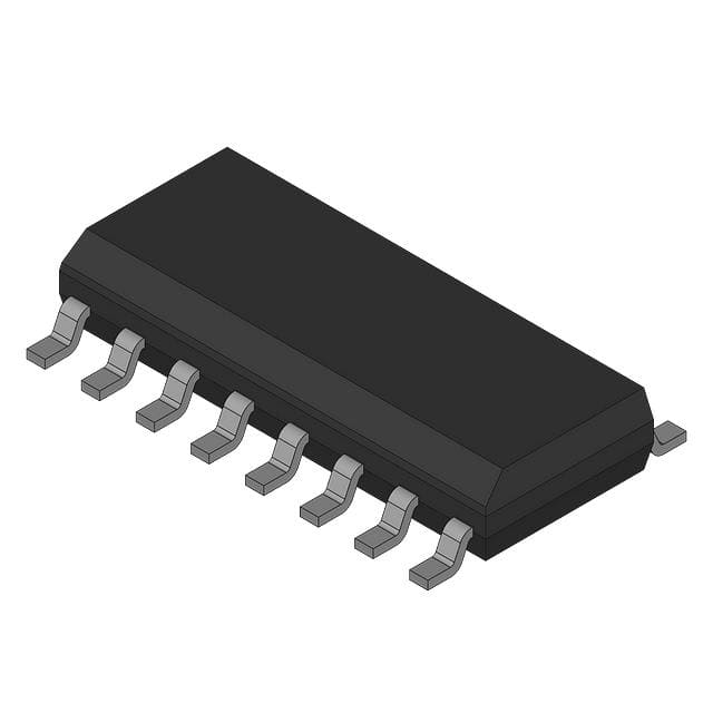
TP13054BDWR is housed in a 16-pin SOIC (DW) package with 1.27 mm pitch, optimized for surface-mount assembly on telecom line cards. Pin functions are electrically and thermally isolated per TI SCTS042A Rev. July 1996.
| Pin/Terminal | Circuit Role | Design Meaning |
|---|---|---|
| VBB (Pin 1) | Negative analog supply | –5 V rail; must be stable and low-noise; connects to analog ground via local decoupling |
| ANLG GND (Pin 2) | Analog reference ground | Separate from digital ground; all analog signals referenced here to minimize noise coupling |
| VFRO (Pin 3) | Receive filter analog output | Low-impedance buffered output (1–3 Ω); drives 600 Ω loads or op-amp inputs directly |
| VCC (Pin 4) | Positive analog supply | +5 V rail; supplies analog core, DAC, and filters; requires 0.1 µF ceramic bypass |
| FSR (Pin 5) | Receive frame-sync input | 8 kHz pulse train; triggers latching of PCM data into DR on falling edge of BCLKR |
| DR (Pin 6) | Receive serial data input | PCM data stream input; sampled on falling edge of BCLKR after FSR leading edge |
| BCLKR/CLKSEL (Pin 7) | Bit clock input / clock select | In sync mode: logic input selecting 1.536/1.544 MHz vs. 2.048 MHz master clock |
| MCLKR/PDN (Pin 8) | Receive master clock / power-down | Low = active; high = power-down (3 mW standby); also accepts 1.536/1.544/2.048 MHz clock |
| MCLKX (Pin 9) | Transmit master clock | Primary timing source for encode path; must be 1.536/1.544/2.048 MHz; asynchronous to MCLKR allowed |
| BCLKX (Pin 10) | Transmit bit clock | Shifts PCM data out on DX; 64 kHz–2.048 MHz, synchronous to MCLKX in sync mode |
| DX (Pin 11) | Transmit serial data output | 3-state PCM output; enabled by FSX; outputs sign-bit first on rising edge of BCLKX |
| FSX (Pin 12) | Transmit frame-sync input | 8 kHz pulse train; initiates encoding cycle; enables DX output buffer on rising edge |
| TSX (Pin 13) | Transmit slot indicator | Open-drain pulse low during encoder time slot; used for external timing synchronization |
| GSX (Pin 14) | Transmit amplifier gain sense | Analog output of transmit input amplifier; used with external resistor network to set gain |
| VFXI+ (Pin 16) | Transmit non-inverting input | High-impedance (+10 MΩ) differential input for voice signal; ±2.5 V common-mode range |
| VFXI– (Pin 15) | Transmit inverting input | Differential complement to VFXI+; enables balanced input configuration and common-mode rejection |
Key Features
| Feature | Design Value |
|---|---|
| Integrated µ-law PCM codec + analog filters | Eliminates need for discrete op-amps, RC networks, and external voltage references - reduces BOM count by ≥12 components |
| Industrial temperature range (–40°C to +85°C) | Enables deployment in uncontrolled environments such as remote DSLAMs, base station cabinets, and outdoor fiber nodes |
| Automatic power-down mode (3 mW) | Reduces thermal load and system power budget during idle periods without firmware intervention |
| Short- and long-frame sync support | Interoperates with legacy T1 (short-frame) and modern E1/T1 hybrid (long-frame) timing architectures |
| Patented low-idle-noise transmit circuitry | Achieves ≤9 dBrnC₀ noise floor - critical for meeting GR-909 Class A line interface specifications |
| Pin-for-pin compatible with TP3054B | Enables drop-in replacement in existing National Semiconductor-based designs with no PCB changes required |
Applications
| T1 Line Interface Card | PABX Subscriber Line Card |
|---|---|
Use Scenario: Digital termination of 2-wire analog telephone lines in carrier-class T1 multiplexers. IC Role / Device Role / Timing Role: Performs A/D conversion, transmit filtering, receive filtering, and D/A conversion - serves as the sole analog front-end for each voice channel. Use Value: Delivers ±0.15 dB gain flatness and <40 µs envelope delay variation to meet GR-303 and TR-NWT-000303 jitter and distortion requirements. |
Use Scenario: Voice channel interface in enterprise private branch exchange systems supporting 24–96 ports. IC Role / Device Role / Timing Role: Codec and filter for subscriber loop signaling, DTMF detection, and voice digitization at 64 kbps. Use Value: µ-law compliance and –40°C to +85°C rating ensure interoperability with PSTN and reliability in non-climate-controlled wiring closets. |
| Digital Encryption Terminal | Voice-Band Data Storage System |
Use Scenario: Secure voice transmission endpoint where encrypted PCM data is processed before analog reconstruction. IC Role / Device Role / Timing Role: Provides clean analog reconstruction (D/A) and anti-aliasing filtering for decrypted PCM streams. Use Value: Low receive noise (4 dBrnC₀) and precise (sin x)/x correction preserve SNR integrity through encryption/decryption cycles. |
Use Scenario: Digitized voice archiving in call-center recording systems using PCM storage buffers. IC Role / Device Role / Timing Role: High-fidelity analog-to-digital capture with transmit-side high-pass filtering to suppress DC and low-frequency hum. Use Value: Integrated active RC noise filters and autozero circuitry reduce baseline drift and 60 Hz interference without external components. |
Equivalent & Alternatives
The following parts are listed as comparable options for similar PCM codec and filter applications.
| Alternative Part | Technical Difference | Application Difference | Selection Advice |
|---|---|---|---|
| TP3054BDWR | Commercial temperature range (0°C to 70°C); identical pinout, µ-law, and electrical specs except temp grade | Restricted to climate-controlled central office or lab environments; not suitable for outdoor or industrial enclosures | Select TP3054BDWR only when ambient operating temperature remains within 0–70°C and cost sensitivity outweighs field-reliability requirements. |
| TP13057BDWR | A-law compliant instead of µ-law; otherwise identical industrial temp rating, package, and timing architecture | Required for E1-based systems (Europe, Asia) and ITU-T G.711 A-law infrastructure; incompatible with µ-law PCM streams | Choose TP13057BDWR exclusively for A-law deployments - no software or hardware adaptation compensates for law mismatch. |
Compared with TP3054BDWR, TP13054BDWR provides extended thermal resilience for field-deployed telecom gear, while TP13057BDWR shifts compliance to A-law ecosystems - neither offers µ-law functionality at industrial temperature without the TP13054BDWR's specific combination of law, grade, and pinout.
Availability
TP13054BDWR is available at Aetrix Electronics and suitable for T1 line interface cards, PABX subscriber line concentrators, and digital encryption terminals requiring stable component supply across extended temperature ranges and long production lifecycles.
Supply support for TP13054BDWR includes scheduled delivery planning, volume procurement assistance, BOM continuity management, traceable sourcing, and lifecycle availability coordination for OEM customers, industrial embedded developers, connected-device designers, and electronics production programs.
Manufacturer
Texas Instruments is a global semiconductor leader specializing in analog, embedded processing, and connectivity solutions for industrial, automotive, and communications markets.
The TP13054BDWR belongs to TI's legacy telecom codec portfolio, engineered specifically for high-density, low-power, µ-law-compliant voice channel termination in carrier and enterprise telephony infrastructure.
FAQ
What is the operating temperature range of the TP13054BDWR?
The TP13054BDWR is specified for operation from –40°C to +85°C. This industrial temperature grade enables reliable deployment in uncontrolled environments such as roadside cabinets, remote DSLAMs, and outdoor wireless base stations - unlike the commercial-grade TP3054BDWR (0°C to 70°C). All electrical parameters in the TI SCTS042A datasheet are guaranteed across this full range.
Does the TP13054BDWR support both short-frame and long-frame sync modes?
Yes, the TP13054BDWR supports both short-frame and long-frame synchronization. On power-up, it defaults to short-frame mode (1-bit-wide FSX/FSR pulses), but automatically detects long-frame pulses (≥3 bit clocks) and adapts timing accordingly. This dual-mode capability ensures interoperability with legacy T1 systems and modern hybrid TDM architectures without hardware modification.
What is the significance of the "DWR" suffix in TP13054BDWR?
The "DWR" suffix denotes a 16-pin SOIC package (DW) with tape-and-reel packaging (R) - standard for automated SMT assembly. The DW package has 1.27 mm lead pitch and meets JEDEC MS-012 specifications. This is the only package variant documented for TP13054B in TI's SCTS042A datasheet; no ceramic or chip-scale variants exist for this part number.
Can the TP13054BDWR be used in A-law PCM systems?
No, the TP13054BDWR is µ-law only. For A-law applications, TI specifies the TP13057BDWR - an identical industrial-grade device with A-law encoding/decoding. Attempting to use TP13054BDWR in an A-law system results in severe quantization distortion and failed interoperation with ITU-T G.711 A-law infrastructure. The law type is hardwired and not user-configurable.
How does the TP13054BDWR achieve low transmit idle noise?
The TP13054BDWR incorporates patented circuitry that actively suppresses idle-channel noise to ≤9 dBrnC₀, meeting Telcordia GR-909 Class A requirements. This is achieved through optimized autozero calibration, precision internal voltage reference, and dedicated active RC noise filters - not merely through external component selection. However, TI cautions against use when composite transmit signals fall below –55 dBm0.
TP13054BDWR Specifications
- Product attributes
- Attribute value
- Manufacturer:
- Texas Instruments
- Series:
- *
- Package/Case:
- -
- Packaging:
- Bulk
- Product Status:
- Active
- Type:
- -
- Data Interface:
- -
- Resolution (Bits):
- -
- Number of ADCs / DACs:
- -
- Sigma Delta:
- -
- S/N Ratio, ADCs / DACs (db) Typ:
- -
- Dynamic Range, ADCs / DACs (db) Typ:
- -
- Voltage - Supply, Analog:
- -
- Voltage - Supply, Digital:
- -
- Operating Temperature:
- -
- Grade:
- -
- Qualification:
- -
- Mounting Type:
- -
- Supplier Device Package:
- -
TP13054BDWR FAQ
1.How can I place an order for TP13054BDWR through Aetrix?
Please submit a Request for Quotation (RFQ) for TP13054BDWR on Aetrix. Our sales agent will provide a competitive quotation and guide you through the order confirmation once you accept the terms.
2.Are the price and stock information for TP13054BDWR reliable?
The price and inventory of TP13054BDWR are updated periodically and may fluctuate due to market conditions. Stock and pricing data are typically refreshed every 24 hours. Quotation validity for TP13054BDWR is usually 5 days.
3.What payment methods are accepted for TP13054BDWR?
We accept Wire Transfer, PayPal, Credit Card, Western Union, MoneyGram, and Escrow for TP13054BDWR transactions.
Note: Certain payment methods may incur a processing fee.
4.How is shipping managed for TP13054BDWR?
TP13054BDWR orders can be shipped via leading logistics carriers, including DHL, UPS, FedEx, TNT, or Registered Mail.
Once your TP13054BDWR order is processed, you will receive an email with the shipment details and tracking number.
Note: Tracking information may take up to 24 hours to appear. Express delivery typically takes 3–5 business days.
5.How can I obtain technical support or documentation for TP13054BDWR?
For technical support, including TP13054BDWR datasheets, pinout diagrams, or application guidance, please contact our engineering support team. They can provide detailed documentation and assistance for your TP13054BDWR requirements.
6.How does Aetrix verify that TP13054BDWR is sourced from the original manufacturer or authorized distributors?
All TP13054BDWR products on Aetrix are procured from qualified distributors and authorized channels. Our dedicated quality assurance team conducts strict verification, including traceability checks and, if necessary, third-party testing. This ensures that TP13054BDWR meets industry standards.
7.What is the process for return or replacement of TP13054BDWR?
All TP13054BDWR units undergo pre-shipment inspection (PSI). If there is an issue with TP13054BDWR, returns or replacements are accepted under the following conditions:
1.Quantity discrepancies, incorrect items, or visible external defects (such as breakage or corrosion), acknowledged by Aetrix.
2.The issue is reported within 90 days of delivery.
3.The TP13054BDWR part is unused and in its original packaging.
Return procedure for TP13054BDWR:
1.Submit a request within 90 days.
2.Obtain a Return Material Authorization (RMA) from Aetrix.
TP13054BDWR Tags
-
NAU88C22YG
Nuvoton Technology Corporation

-
TLV320AIC3100IRHBR
Texas Instruments
-
DA7212-01UM2
Renesas
-
NAU8810YG
Nuvoton Technology Corporation
-
DA7218-00U32
Renesas
-
CMX655DQ6-TR1K
CML Micro
-
SGTL5000XNLA3
NXP Semiconductors
-
TLV320AIC3104IRHBR
Texas Instruments
-
MAX9867EWV+T
Analog Devices Inc./Maxim Integrated

-
MAX9860ETG+T
Analog Devices Inc./Maxim Integrated

-
TLV320AIC3106IRGZR
Texas Instruments
-
SGTL5000XNLA3R2
NXP Semiconductors
Tech Hub

A practical engineering guide to 3.3V and 5V logic compatibility, input thresholds, resistor dividers, translator ICs, MOSFET level shifting, I2C pull-ups, timing limits and power-sequencing risks.

The 74HC595 uses push-pull logic outputs, while the TPIC6B595 uses 50 V open-drain DMOS sinks for higher-power loads. This guide compares timing, current limits, 3.3 V interfacing, load wiring, thermal…

The 74HC595 converts serial data into eight stable parallel outputs. This guide covers pin functions, shift and storage timing, OE and MR behavior, drive-current limits, cascading, voltage compatibilit…

A technical comparison of level-sensitive latches and edge-triggered flip-flops, covering timing windows, setup and hold limits, master–slave operation, time borrowing, race-through, HDL inference and…

A D latch stores one bit while Enable controls when data can pass. This reference covers gate-level operation, truth tables, transparency, setup and hold timing, LE versus OE, common ICs and practical …

An SR latch stores one bit through cross-coupled feedback. This engineering reference covers NOR and NAND implementations, truth tables, forbidden-state recovery, gated operation, switch debouncing, fa…

Latch circuits retain one bit through feedback. This technical reference covers SR and D latches, truth tables, transparency, timing limits, latch-versus-flip-flop behavior, applications and common log…

An engineering guide to LED driver operation, constant-current and constant-voltage outputs, linear and switching topologies, dimming, IC selection, calculations, replacement compatibility, and fault c…

Operational amplifier guide covering op amp basics, feedback, ideal vs real op amps, common configurations, buffer circuits, offset, bias current, gain-bandwidth, slew rate, rail-to-rail limits and sel…

Jumper cables guide covering safe connection order, red and black clamp placement, final ground connection, cable gauge, length, clamp quality, copper vs CCA cables, jump starter comparison and battery…


