
 My Inquiry
 My Account


Texas Instruments TP3057ADWR
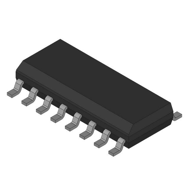
- Part No.:
- TP3057ADWR
- Manufacturer:
- Texas Instruments
- Category:
- CODECS
- Package:
- -
- Datasheet:
-
 TP3057ADWR.pdf
- Description:
- PCM CODEC, A-LAW, 1-FUNC, CMOS
- Quantity:
- Payment:

- Shipping:

Inventory:6,000
Please send an inquiry. Send us your inquiry, and we will respond immediately.
Product details
Overview
TP3057ADWR from Texas Instruments is an A-law compatible monolithic PCM codec and filter IC designed for full-duplex voice telephony interface in TDM systems. It integrates transmit A/D conversion, receive D/A conversion, active RC noise filtering, (sin x)/x correction, and internal precision voltage reference. Operates at ±5 V, consumes 9 mA typical supply current in active mode, and supports 1.536/1.544/2.048 MHz master clocks - used in T1 carrier line interface cards and digital PABX systems.
For engineers reviewing the TP3057ADWR datasheet, TP3057ADWR pinout, TP3057ADWR application, or TP3057ADWR equivalent, this device requires attention to its A-law encoding compliance, psophometric-weighted noise performance (–75 dBm0p), power-down control via MCLKR/PDN, and strict short- or long-frame sync timing constraints for frame-synchronized PCM data transfer.
Technical Context
The TP3057ADWR implements a complete analog-to-digital and digital-to-analog signal path with integrated switched-capacitor band-pass filtering on transmit and low-pass filtering with (sin x)/x compensation on receive. Its architecture includes autozero circuitry for offset stability and TTL/CMOS-compatible serial I/O supporting both synchronous and asynchronous clocking modes.
It uses dual master clocks (MCLKX/MCLKR) and separate frame-sync (FSX/FSR) and bit-clock (BCLKX/BCLKR) signals to manage time-division multiplexed PCM streams. The transmit section features patented low-idle-noise circuitry optimized for A-law systems but not recommended below –55 dBm0 composite signal levels.
Key Specifications
| Parameter | Value and Actual Design Meaning |
|---|---|
| A-law encoding | Complies with CCITT G.711 A-law standard for 8-bit PCM quantization - ensures interoperability with European and global digital telephony infrastructure. |
| Psophometric noise (Tx) | –75 dBm0p typical - meets stringent voice-band noise requirements for carrier-grade line interface applications. |
| Supply voltage | ±5 V ±5% - requires dual-rail analog supply; VCC = +5 V, VBB = –5 V; incompatible with single-supply operation. |
| Operating temperature | 0°C to 70°C - specified for commercial-grade deployment in central office and enterprise telecom equipment. |
| Power consumption | 9 mA typical ICC/IBB in active mode, 1 mA in power-down - enables thermal management in high-density line card designs. |
| Master clock support | 1.536 MHz, 1.544 MHz, or 2.048 MHz - selectable via BCLKR/CLKSEL logic input; supports T1 (1.544 MHz) and E1 (2.048 MHz) standards. |
| Frame sync modes | Short-frame (1-bit pulse) or long-frame (3–8 bit pulses) - determines timing alignment strategy for PCM time slots in TDM frames. |
Pinout & Package
TP3057ADWR is housed in a 16-pin SOIC (DW) package with gull-wing leads, 1.27 mm pitch, and moisture sensitivity level (MSL) 3 per JEDEC J-STD-020. Pin numbering follows standard top-view orientation with Pin 1 at bottom-left corner.
| Pin/Terminal | Circuit Role | Design Meaning |
|---|---|---|
| VBB | Negative analog supply | –5 V ±5% rail; powers analog sections including codec core and filters; must be stable and low-noise. |
| ANLG GND | Analog ground reference | Common return for all analog signals; must be isolated from digital ground to prevent noise coupling. |
| VFRO | Receive filter analog output | Low-impedance buffered output of receive low-pass filter; drives external hybrid or amplifier stage. |
| VCC | Positive analog supply | +5 V ±5% rail; powers analog circuits; decoupling required near pin for transient suppression. |
| FSR | Receive frame sync input | 8 kHz pulse train triggering PCM data capture into DR; rising edge initiates sampling sequence. |
| DR | Receive serial data input | PCM data stream latched on falling edge of BCLKR; synchronous with FSR and bit clock. |
| BCLKR/CLKSEL | Bit clock input / clock select | In sync mode: selects 1.536/1.544 MHz vs. 2.048 MHz master clock; in async mode: serves as receive bit clock. |
| MCLKR/PDN | Receive master clock / power-down control | Low = active; high = power-down; floating or high disables internal clocks and places DX/VFRO in high-Z. |
| VFXI+ | Transmit amplifier non-inverting input | Primary analog voice input; accepts ±2.5 V common-mode range; high-impedance (10 MΩ) interface. |
| VFXI– | Transmit amplifier inverting input | Differential input pair with VFXI+; enables balanced signal conditioning and gain setting via GSX feedback. |
| GSX | Transmit amplifier output | Open-loop output used to set gain externally; drives 10 kΩ load with ±2.8 V dynamic range. |
| TSX | Encoder time-slot indicator | Open-drain output pulsed low during encoder time slot; used for external timing synchronization or monitoring. |
| FSX | Transmit frame sync input | 8 kHz pulse train enabling PCM data output on DX; rising edge triggers transmit encoding cycle. |
| DX | Transmit serial data output | 3-state PCM output enabled by FSX; data shifted out on rising edge of BCLKX; high-Z when disabled. |
| BCLKX | Transmit bit clock input | 64 kHz–2.048 MHz clock synchronizing PCM data output on DX; must be synchronous with MCLKX in sync mode. |
| MCLKX | Transmit master clock input | 1.536/1.544/2.048 MHz clock driving internal timing; selected as sole master clock when MCLKR/PDN is high. |
Key Features
| Feature | Design Value |
|---|---|
| A-law + psophometric optimization | Delivers –75 dBm0p transmit noise floor - meets ITU-T P.51 and ETSI EN 300 019 requirements for voiceband clarity in European telecom systems. |
| Integrated (sin x)/x correction | Compensates for DAC zero-order hold droop in receive path - maintains flat frequency response from 300 Hz to 3400 Hz within ±0.15 dB. |
| Autozero circuitry | Reduces input offset drift over temperature and time - keeps VIO ≤ ±20 mV across 0°C–70°C, critical for consistent gain tracking. |
| Programmable sync/asynchronous operation | Supports both clock domains: synchronous (shared MCLKX) or asynchronous (independent MCLKX/MCLKR) - enables flexible integration into legacy and new TDM backplanes. |
| Power-down mode (3 mW) | Reduces total dissipation to <1 mW active current draw - allows selective channel shutdown in multi-channel line cards without PCB layout changes. |
Applications
| Line Interface Card (LIC) | Digital PABX System |
|---|---|
Use Scenario: Installed on a T1/E1 line card to terminate analog subscriber loops and convert voice signals to 64 kbps PCM channels. IC Role / Device Role / Timing Role: Performs full-duplex A-law PCM encoding/decoding, transmit/receive filtering, and frame-aligned serial I/O interfacing with TDM switch fabric. Use Value: Enables 24–30 simultaneous voice channels per card with <–75 dBm0p transmit noise and <–83 dBm0p receive noise - meeting GR-909 and Telcordia CS-2 compliance. |
Use Scenario: Embedded in digital private branch exchange hardware to interface analog station ports with digital switching matrix. IC Role / Device Role / Timing Role: Acts as channelized voice interface with independent FSX/FSR timing, supporting both short- and long-frame sync for mixed vendor interoperation. Use Value: Provides precise gain tracking (±0.25 dB over –40 dBm0 to +3 dBm0) and crosstalk isolation >–75 dB - ensuring clear call quality across distributed extension sets. |
| Central Office Terminal | Digital Voice Encryption Module |
Use Scenario: Used in Class 5 central office line termination units to digitize analog trunk lines before routing through SS7/IP core networks. IC Role / Device Role / Timing Role: Serves as analog front-end with internal voltage reference and RC noise filtering - eliminates need for external precision references or op-amp filters. Use Value: Delivers envelope delay distortion <40 µs peak-to-peak across 500–1600 Hz - satisfying ITU-T G.113 Annex A limits for end-to-end talker echo control. |
Use Scenario: Integrated into secure voice encryption devices where analog voice is digitized prior to AES-256 encryption and packetization. IC Role / Device Role / Timing Role: Provides deterministic, low-jitter PCM sampling synchronized to crypto engine clock domain via programmable frame sync. Use Value: Maintains <–90 dB transmit-to-receive crosstalk and <–46 dB single-frequency distortion - preserving signal integrity for post-encryption spectral analysis. |
Equivalent & Alternatives
The following parts are listed as comparable options for similar PCM codec and filter applications.
| Alternative Part | Technical Difference | Application Difference | Selection Advice |
|---|---|---|---|
| TP3057N | Same A-law functionality and pinout, but in 16-pin PDIP (N) package - larger footprint, higher thermal resistance (9.2 mW/°C derating). | Preferred for prototyping or low-volume industrial boards where SOIC reflow is unavailable; unsuitable for high-density telecom line cards. | Select TP3057N only if manual soldering or socket-based validation is required; TP3057ADWR offers superior thermal performance and board space efficiency. |
| MC145506P | A-law codec without integrated filtering; requires external RC or switched-capacitor filters; no (sin x)/x correction; higher transmit noise (–65 dBm0p). | Suitable for cost-sensitive, non-carrier applications where filter performance is relaxed; lacks autozero and precision internal reference. | Choose MC145506P only for legacy designs or budget-constrained embedded voice recorders - not for T1/E1 line interface where filtering and noise specs are mandatory. |
Compared with TP3057N and MC145506P, TP3057ADWR delivers integrated filtering, lower noise, and SOIC packaging optimized for telecom line card density - making it the only option that satisfies full GR-909-compliant A-law interface requirements without external components.
Availability
TP3057ADWR is available at Aetrix Electronics and suitable for T1 carrier line interface cards, digital PABX systems, and central office terminal equipment requiring stable component supply and long-term lifecycle support.
Supply support for TP3057ADWR includes scheduled delivery planning, volume procurement assistance, BOM continuity management, traceable sourcing, and lifecycle availability coordination for OEM customers, industrial embedded developers, connected-device designers, and electronics production programs.
Manufacturer
Texas Instruments is a global semiconductor leader specializing in analog, embedded processing, and connectivity solutions for industrial, automotive, and communications markets.
The TP3057ADWR belongs to TI's legacy telecom interface product line, engineered specifically for A-law PCM digitization in carrier-class voice infrastructure - emphasizing noise performance, timing precision, and reliability under continuous operation.
FAQ
What is the primary function of the TP3057ADWR in a TDM system?
The TP3057ADWR performs full-duplex A-law PCM encoding and decoding with integrated transmit high-pass/low-pass filtering and receive low-pass filtering featuring (sin x)/x correction. In a TDM system, it terminates analog voice lines and converts them to/from 64 kbps PCM streams synchronized to FSX/FSR frame pulses - enabling direct connection to time-division multiplexed switch fabrics without external converters or filters.
Does the TP3057ADWR support both synchronous and asynchronous clocking modes?
Yes, the TP3057ADWR supports both modes. In synchronous mode, MCLKX serves as the master clock for both transmit and receive paths while MCLKR/PDN acts as a power-down control. In asynchronous mode, independent MCLKX and MCLKR clocks drive transmit and receive sections respectively - though best performance is achieved when they are phase-locked. The BCLKR/CLKSEL pin configures master clock selection in sync mode.
What is the significance of the psophometric-weighted noise specification for TP3057ADWR?
The TP3057ADWR specifies –75 dBm0p typical psophometric-weighted transmit noise, reflecting human ear sensitivity weighting centered at 800 Hz. This metric is mandated for A-law systems in European and ITU-regulated telecom networks. Unlike C-message weighting used for µ-law devices, psophometric weighting validates voice clarity under real-world telephone channel conditions - confirming TP3057ADWR compliance with ETSI EN 300 019 and ITU-T P.51.
How does the TP3057ADWR handle power-down sequencing?
The TP3057ADWR enters power-down when MCLKR/PDN is held high, reducing supply current to ~1 mA and placing DX and VFRO in high-impedance states. To avoid latch-up, TI specifies a strict power-up sequence: ground first, then VBB, then VCC, then assert power-down, then apply clocks, then release power-down, then apply FS pulses, then apply analog signals. This sequence prevents parasitic SCR activation in the CMOS process.
Can the TP3057ADWR be used in µ-law systems?
No, the TP3057ADWR is strictly A-law compliant and not interchangeable with µ-law codecs like the TP3054A series. Its internal quantizer, companding law, and psophometric noise measurement are optimized for A-law standards (ITU-T G.711 Annex A). Using TP3057ADWR in a µ-law system would result in severe quantization distortion and failure to meet GR-303 or Telcordia CS-2 voice quality requirements.
TP3057ADWR Specifications
- Product attributes
- Attribute value
- Manufacturer:
- Texas Instruments
- Series:
- *
- Package/Case:
- -
- Packaging:
- Bulk
- Product Status:
- Active
- Type:
- -
- Data Interface:
- -
- Resolution (Bits):
- -
- Number of ADCs / DACs:
- -
- Sigma Delta:
- -
- S/N Ratio, ADCs / DACs (db) Typ:
- -
- Dynamic Range, ADCs / DACs (db) Typ:
- -
- Voltage - Supply, Analog:
- -
- Voltage - Supply, Digital:
- -
- Operating Temperature:
- -
- Grade:
- -
- Qualification:
- -
- Mounting Type:
- -
- Supplier Device Package:
- -
TP3057ADWR FAQ
1.How can I place an order for TP3057ADWR through Aetrix?
Please submit a Request for Quotation (RFQ) for TP3057ADWR on Aetrix. Our sales agent will provide a competitive quotation and guide you through the order confirmation once you accept the terms.
2.Are the price and stock information for TP3057ADWR reliable?
The price and inventory of TP3057ADWR are updated periodically and may fluctuate due to market conditions. Stock and pricing data are typically refreshed every 24 hours. Quotation validity for TP3057ADWR is usually 5 days.
3.What payment methods are accepted for TP3057ADWR?
We accept Wire Transfer, PayPal, Credit Card, Western Union, MoneyGram, and Escrow for TP3057ADWR transactions.
Note: Certain payment methods may incur a processing fee.
4.How is shipping managed for TP3057ADWR?
TP3057ADWR orders can be shipped via leading logistics carriers, including DHL, UPS, FedEx, TNT, or Registered Mail.
Once your TP3057ADWR order is processed, you will receive an email with the shipment details and tracking number.
Note: Tracking information may take up to 24 hours to appear. Express delivery typically takes 3–5 business days.
5.How can I obtain technical support or documentation for TP3057ADWR?
For technical support, including TP3057ADWR datasheets, pinout diagrams, or application guidance, please contact our engineering support team. They can provide detailed documentation and assistance for your TP3057ADWR requirements.
6.How does Aetrix verify that TP3057ADWR is sourced from the original manufacturer or authorized distributors?
All TP3057ADWR products on Aetrix are procured from qualified distributors and authorized channels. Our dedicated quality assurance team conducts strict verification, including traceability checks and, if necessary, third-party testing. This ensures that TP3057ADWR meets industry standards.
7.What is the process for return or replacement of TP3057ADWR?
All TP3057ADWR units undergo pre-shipment inspection (PSI). If there is an issue with TP3057ADWR, returns or replacements are accepted under the following conditions:
1.Quantity discrepancies, incorrect items, or visible external defects (such as breakage or corrosion), acknowledged by Aetrix.
2.The issue is reported within 90 days of delivery.
3.The TP3057ADWR part is unused and in its original packaging.
Return procedure for TP3057ADWR:
1.Submit a request within 90 days.
2.Obtain a Return Material Authorization (RMA) from Aetrix.
TP3057ADWR Tags
-
NAU88C22YG
Nuvoton Technology Corporation

-
TLV320AIC3100IRHBR
Texas Instruments
-
DA7212-01UM2
Renesas
-
NAU8810YG
Nuvoton Technology Corporation
-
DA7218-00U32
Renesas
-
CMX655DQ6-TR1K
CML Micro
-
SGTL5000XNLA3
NXP Semiconductors
-
TLV320AIC3104IRHBR
Texas Instruments
-
MAX9867EWV+T
Analog Devices Inc./Maxim Integrated

-
MAX9860ETG+T
Analog Devices Inc./Maxim Integrated

-
TLV320AIC3106IRGZR
Texas Instruments
-
SGTL5000XNLA3R2
NXP Semiconductors
Tech Hub

A practical engineering guide to 3.3V and 5V logic compatibility, input thresholds, resistor dividers, translator ICs, MOSFET level shifting, I2C pull-ups, timing limits and power-sequencing risks.

The 74HC595 uses push-pull logic outputs, while the TPIC6B595 uses 50 V open-drain DMOS sinks for higher-power loads. This guide compares timing, current limits, 3.3 V interfacing, load wiring, thermal…

The 74HC595 converts serial data into eight stable parallel outputs. This guide covers pin functions, shift and storage timing, OE and MR behavior, drive-current limits, cascading, voltage compatibilit…

A technical comparison of level-sensitive latches and edge-triggered flip-flops, covering timing windows, setup and hold limits, master–slave operation, time borrowing, race-through, HDL inference and…

A D latch stores one bit while Enable controls when data can pass. This reference covers gate-level operation, truth tables, transparency, setup and hold timing, LE versus OE, common ICs and practical …

An SR latch stores one bit through cross-coupled feedback. This engineering reference covers NOR and NAND implementations, truth tables, forbidden-state recovery, gated operation, switch debouncing, fa…

Latch circuits retain one bit through feedback. This technical reference covers SR and D latches, truth tables, transparency, timing limits, latch-versus-flip-flop behavior, applications and common log…

An engineering guide to LED driver operation, constant-current and constant-voltage outputs, linear and switching topologies, dimming, IC selection, calculations, replacement compatibility, and fault c…

Operational amplifier guide covering op amp basics, feedback, ideal vs real op amps, common configurations, buffer circuits, offset, bias current, gain-bandwidth, slew rate, rail-to-rail limits and sel…

Jumper cables guide covering safe connection order, red and black clamp placement, final ground connection, cable gauge, length, clamp quality, copper vs CCA cables, jump starter comparison and battery…


