
 My Inquiry
 My Account


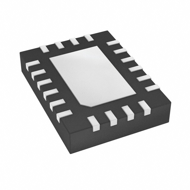
Texas Instruments TPS25940ARVCT
- Part No.:
- TPS25940ARVCT
- Manufacturer:
- Texas Instruments
- Category:
- Current Regulation/Management
- Package:
- 20-WFQFN Exposed Pad
- Datasheet:
-
 TPS25940ARVCT.pdf
- Description:
- IC ELECTRONIC FUSE 8% 20WQFN
- Quantity:
- Payment:

- Shipping:

Inventory:1,137
Please send an inquiry. Send us your inquiry, and we will respond immediately.
Product details
Overview
TPS25940ARVCT from Texas Instruments is a 2.7–18 V eFuse power switch with true reverse current blocking, 42 mΩ typical RON, 0.6–5.3 A adjustable current limit (±8%), IMON current monitor output (±8%), and DevSleep™ mode supporting SATA Device Sleep compliance. It protects SSDs and enterprise storage systems against overcurrent, overvoltage, undervoltage, thermal fault, and reverse voltage events.
For engineers reviewing the TPS25940ARVCT datasheet, TPS25940ARVCT pinout, TPS25940ARVCT application, or TPS25940ARVCT equivalent, key selection considerations include its bidirectional FET architecture for holdup-energy systems, programmable dV/dt ramp control, 95 µA DevSleep IQ, and UL 2367/UL60950 safety recognition.
Technical Context
The TPS25940ARVCT integrates back-to-back N-channel MOSFETs to enable true reverse current blocking-triggering shutdown when V(IN) < V(OUT) – 10 mV-and supports seamless switchover to boosted backup supplies. Its DevSleep mode reduces quiescent current to 95 µA while maintaining fault monitoring via FLT and PGOOD outputs.
Programmable thresholds include ±2% OVP/UVLO, 1 µs reverse-voltage shutoff, and fast-trip comparator activation at 1.5×ILIM + 0.375 A. The device uses external RILIM (16.9–150 kΩ) and CdVdT (0–470 nF) to set current limit and output ramp rate, respectively.
Key Specifications
| Parameter | Value and Actual Design Meaning |
|---|---|
| Input Voltage Range | 2.7 V to 18 V - supports common DC bus rails including 3.3 V, 5 V, 12 V, and 15 V systems without level-shifting. |
| RON (Typical) | 42 mΩ - enables low conduction loss (<500 mW at 3.5 A), reducing thermal stress in high-current SSD power paths. |
| Adjustable ILIM | 0.6 A to 5.3 A (±8%) - set by single resistor RILIM; supports scalable protection across PCIe/SATA SSDs and RAID cards. |
| DevSleep IQ | 95 µA (typical) - meets SATA Device Sleep specification for ultra-low-power idle states in storage subsystems. |
| Reverse Blocking Threshold | V(IN) < V(OUT) – 10 mV - prevents load-side holdup energy from discharging into a failed upstream supply. |
| Protection Outputs | Open-drain FLT (fault) and PGOOD (power-good) - provide direct interface to host controllers for real-time status and sequencing control. |
| UL Recognition | UL 2367 (File No. 169910) and UL60950 - certified safe under single-point failure conditions per safety-critical storage standards. |
Pinout & Package
TPS25940ARVCT is housed in a 20-pin WQFN package (3.00 mm × 4.00 mm) with exposed thermal pad requiring PCB ground connection via multiple vias for optimal thermal performance.
| Pin/Terminal | Circuit Role | Design Meaning |
|---|---|---|
| IN (Pins 9–13) | Power input supply node | Accepts 2.7–18 V input; connects to upstream DC bus or adapter; pins are paralleled for current sharing and low-impedance path. |
| OUT (Pins 4–8) | Switched power output node | Delivers protected power to load; pins are paralleled to reduce trace resistance and improve current handling. |
| EN/UVLO (Pin 14) | Enable and UVLO threshold input | Active-high enable with 0.99 V rising threshold; also sets undervoltage lockout at 2.3 V (rising) with 116 mV hysteresis. |
| OVP (Pin 15) | Overvoltage protection threshold input | Configures OVP trip point at 0.99 V; asserts FLT within 2 µs when exceeded. |
| DEVSLP (Pin 1) | DevSleep mode control | Active-high signal enabling 95 µA low-power state; maintains FLT/PGOOD monitoring during SATA Device Sleep. |
| ILIM (Pin 17) | Current limit programming | Resistor-to-GND sets ILIM from 0.6 A to 5.3 A; open/short configurations support UL60950 single-point failure testing. |
| dVdT (Pin 18) | Output voltage ramp control | Capacitor-to-GND sets soft-start slew rate; gain of 11.9 V/V ensures precise dV/dt control independent of load. |
| IMON (Pin 19) | Analog current monitor output | Sources 52.3 µA/A (±8%) proportional to load current; enables real-time current measurement with external resistor. |
| PGTH (Pin 3) | Power-good threshold input | Sets PGOOD assertion threshold at 0.99 V; used to define valid output voltage window for downstream logic. |
| FLT (Pin 20) | Fault indicator output | Open-drain active-low flag signaling UVLO, OVP, reverse voltage, thermal shutdown, or fast-trip events. |
| PGOOD (Pin 2) | Power-good status output | Open-drain active-high output with 0.54 ms de-glitch delay; indicates stable regulated output meeting PGTH threshold. |
| GND (Pin 16) | System ground reference | Must be connected to PCB ground plane; thermal pad requires dedicated vias for junction-to-board thermal resistance of 13.6 °C/W. |
Key Features
| Feature | Design Value |
|---|---|
| True reverse current blocking | Shuts off within 1 µs when V(IN) drops below V(OUT) – 10 mV - prevents backfeed from load-side capacitors into failed supplies. |
| Programmable dV/dt ramp control | External capacitor sets output slew rate with 11.9 V/V gain - eliminates inrush current spikes during hot-plug or power-up in SSDs. |
| Integrated IMON current monitor | 52.3 µA/A output with ±8% accuracy - enables precision load-current telemetry without external sense resistors or amplifiers. |
| UL 2367 and UL60950 recognition | Validated for single-point failure safety - allows use in enterprise storage where fault containment and fire-risk mitigation are mandatory. |
| DevSleep™ mode with fault visibility | 95 µA quiescent current while retaining FLT and PGOOD monitoring - satisfies SATA Device Sleep spec without sacrificing system-level fault awareness. |
Applications
| PCIe/SATA SSD Power Management | RAID Card Holdup Power Control |
|---|---|
Use Scenario: Power delivery to NVMe or SATA SSDs in servers and workstations where bus voltage may collapse while load-side bulk capacitance remains charged. IC Role / Device Role / Timing Role: eFuse controller providing reverse-blocking, current limiting, and soft-start during hot-swap or recovery sequences. Use Value: Prevents uncontrolled discharge of 10–100 mF holdup capacitors into failed 12 V rails, avoiding system instability and component overstress. | Use Scenario: Managing redundant power paths in multi-drive RAID enclosures with backup supercapacitors or battery-backed modules. IC Role / Device Role / Timing Role: Bidirectional power switch enabling automatic switchover from main rail to backup source when V(IN) falls below V(OUT) – 10 mV. Use Value: Achieves sub-millisecond reverse-shutoff and seamless transition - critical for maintaining data integrity during brief AC outages. |
| Enterprise Server Backplane Protection | SATA Device Sleep Compliance |
Use Scenario: Protecting hot-pluggable drive bays on server backplanes subject to ESD, short circuits, and voltage transients. IC Role / Device Role / Timing Role: Primary overcurrent and overvoltage protector with 2 µs OVP response and 200 ns fast-trip detection. Use Value: Limits fault energy to <100 mJ during short-circuit events - prevents damage to backplane traces and neighboring components. | Use Scenario: Enabling ultra-low-power idle states in client and enterprise SSDs compliant with SATA Rev. 3.3 Device Sleep standard. IC Role / Device Role / Timing Role: Low-IQ power switch maintaining fault monitoring capability during DevSleep mode. Use Value: Reduces standby power to ≤95 µA while preserving FLT assertion on thermal or overvoltage faults - extends battery life in portable storage. |
Equivalent & Alternatives
The following parts are listed as comparable options for similar eFuse power switch applications.
| Alternative Part | Technical Difference | Application Difference | Selection Advice |
|---|---|---|---|
| TPS25940L RVCT | Latched fault response (vs. auto-retry in TPS25940ARVCT); identical pinout, RON, and protection features. | Preferred in systems requiring manual reset after fault to prevent uncontrolled re-enabling during persistent faults. | Select TPS25940L RVCT when fault persistence must halt operation until host intervention; otherwise retain TPS25940ARVCT for self-recovering behavior. |
| TPS259621RGER | Higher 60 V max input, lower 18 mΩ RON, but no DevSleep mode or UL 2367 certification; different pinout and package (24-pin VQFN). | Suitable for industrial 24/48 V systems needing higher voltage tolerance, but not for SATA-compliant SSDs requiring DevSleep or safety recognition. | Choose TPS259621RGER only for non-storage 60 V applications; TPS25940ARVCT remains optimal for SATA/PCIe SSDs with safety and low-power requirements. |
Compared with TPS25940L RVCT, the TPS25940ARVCT provides auto-retry fault recovery ideal for transient overload scenarios in SSDs; versus TPS259621RGER, it delivers certified DevSleep operation and UL safety compliance essential for enterprise storage qualification - neither alternative matches both functional and regulatory scope.
Availability
TPS25940ARVCT is available at Aetrix Electronics and suitable for PCIe/SATA SSD drives, enterprise server backplanes, and RAID card holdup power management requiring stable component supply, long-term lifecycle support, and full safety certification.
Supply support for TPS25940ARVCT includes scheduled delivery planning, volume procurement assistance, BOM continuity management, traceable sourcing, and lifecycle availability coordination for OEM customers, industrial embedded developers, connected-device designers, and electronics production programs.
Manufacturer
Texas Instruments is a global semiconductor leader delivering analog, embedded processing, and connectivity solutions for industrial, automotive, and communications markets.
The TPS25940x family is designed specifically for high-reliability storage power management, integrating reverse blocking, DevSleep, and safety-certified protection in compact WQFN packages for SSDs and enterprise servers.
FAQ
What is the maximum input voltage rating for the TPS25940ARVCT?
The TPS25940ARVCT has an absolute maximum input voltage rating of 20 V, with recommended operating range from 2.7 V to 18 V. Transient input excursions up to 22 V are allowed for durations ≤10 ms. This rating enables robust operation across 12 V server rails and 15 V industrial supplies while maintaining margin against line surges.
How does the TPS25940ARVCT implement true reverse current blocking?
The TPS25940ARVCT implements true reverse current blocking using internal comparators that continuously monitor V(IN) – V(OUT). When this differential falls below –10 mV (with –9.3 mV typical threshold), the device disables both back-to-back FETs within 1 µs. This prevents load-side holdup energy from discharging into a failed or disconnected upstream supply - a critical function in SSDs with large output capacitance.
What is the purpose of the DEVSLP pin on the TPS25940ARVCT?
The DEVSLP pin on the TPS25940ARVCT is an active-high control input that enables DevSleep™ mode, reducing quiescent current to 95 µA (typical) while maintaining FLT and PGOOD monitoring capability. This function directly supports SATA Device Sleep compliance for ultra-low-power idle states in client and enterprise SSDs without sacrificing fault visibility.
Can the TPS25940ARVCT be used in systems requiring UL safety certification?
Yes, the TPS25940ARVCT is UL 2367 Recognized (File No. 169910) and UL60950 certified for safe operation during single-point failure conditions. These certifications validate its ability to contain faults - such as open/short ILIM resistor failures - without fire hazard or electric shock risk, making it suitable for safety-critical enterprise storage applications.
How is the current limit programmed on the TPS25940ARVCT?
The current limit on the TPS25940ARVCT is programmed using a single external resistor (RILIM) connected from Pin 17 (ILIM) to GND. Values from 16.9 kΩ to 150 kΩ set ILIM from 4.81 A down to 0.6 A, with ±8% accuracy. Open and short configurations are supported for UL60950 single-point failure testing, yielding 0.45 A and 0.67 A limits respectively.
TPS25940ARVCT Specifications
- Product attributes
- Attribute value
- Manufacturer:
- Texas Instruments
- Series:
- -
- Package/Case:
- 20-WFQFN Exposed Pad
- Packaging:
- Tape & Reel (TR)
- Product Status:
- Active
- Function:
- Electronic Fuse
- Sensing Method:
- -
- Accuracy:
- ±8%
- Voltage - Input:
- 2.7V ~ 18V
- Current - Output:
- 5.3A
- Operating Temperature:
- -40°C ~ 125°C (TJ)
- Grade:
- -
- Qualification:
- -
- Mounting Type:
- Surface Mount
- Supplier Device Package:
- 20-WQFN (4x3)
TPS25940ARVCT FAQ
1.How can I place an order for TPS25940ARVCT through Aetrix?
Please submit a Request for Quotation (RFQ) for TPS25940ARVCT on Aetrix. Our sales agent will provide a competitive quotation and guide you through the order confirmation once you accept the terms.
2.Are the price and stock information for TPS25940ARVCT reliable?
The price and inventory of TPS25940ARVCT are updated periodically and may fluctuate due to market conditions. Stock and pricing data are typically refreshed every 24 hours. Quotation validity for TPS25940ARVCT is usually 5 days.
3.What payment methods are accepted for TPS25940ARVCT?
We accept Wire Transfer, PayPal, Credit Card, Western Union, MoneyGram, and Escrow for TPS25940ARVCT transactions.
Note: Certain payment methods may incur a processing fee.
4.How is shipping managed for TPS25940ARVCT?
TPS25940ARVCT orders can be shipped via leading logistics carriers, including DHL, UPS, FedEx, TNT, or Registered Mail.
Once your TPS25940ARVCT order is processed, you will receive an email with the shipment details and tracking number.
Note: Tracking information may take up to 24 hours to appear. Express delivery typically takes 3–5 business days.
5.How can I obtain technical support or documentation for TPS25940ARVCT?
For technical support, including TPS25940ARVCT datasheets, pinout diagrams, or application guidance, please contact our engineering support team. They can provide detailed documentation and assistance for your TPS25940ARVCT requirements.
6.How does Aetrix verify that TPS25940ARVCT is sourced from the original manufacturer or authorized distributors?
All TPS25940ARVCT products on Aetrix are procured from qualified distributors and authorized channels. Our dedicated quality assurance team conducts strict verification, including traceability checks and, if necessary, third-party testing. This ensures that TPS25940ARVCT meets industry standards.
7.What is the process for return or replacement of TPS25940ARVCT?
All TPS25940ARVCT units undergo pre-shipment inspection (PSI). If there is an issue with TPS25940ARVCT, returns or replacements are accepted under the following conditions:
1.Quantity discrepancies, incorrect items, or visible external defects (such as breakage or corrosion), acknowledged by Aetrix.
2.The issue is reported within 90 days of delivery.
3.The TPS25940ARVCT part is unused and in its original packaging.
Return procedure for TPS25940ARVCT:
1.Submit a request within 90 days.
2.Obtain a Return Material Authorization (RMA) from Aetrix.
TPS25940ARVCT Tags
.jpg)
-
PSSI2021SAY,115
Nexperia USA Inc.

-
BCR401RE6327HTSA1
Infineon Technologies

-
INA199B2DCKR
Texas Instruments
-
INA199A1DCKR
Texas Instruments
-
INA199B1DCKR
Texas Instruments
-
NSI45015WT1G
onsemi
-
NSI45020T1G
onsemi
-
NSI45030AT1G
onsemi
-
NSI45025AT1G
onsemi
-
NSI45020AT1G
onsemi
-
NSI50010YT1G
onsemi
-
LM334Z/NOPB
Texas Instruments
Tech Hub

A practical engineering guide to 3.3V and 5V logic compatibility, input thresholds, resistor dividers, translator ICs, MOSFET level shifting, I2C pull-ups, timing limits and power-sequencing risks.

The 74HC595 uses push-pull logic outputs, while the TPIC6B595 uses 50 V open-drain DMOS sinks for higher-power loads. This guide compares timing, current limits, 3.3 V interfacing, load wiring, thermal…

The 74HC595 converts serial data into eight stable parallel outputs. This guide covers pin functions, shift and storage timing, OE and MR behavior, drive-current limits, cascading, voltage compatibilit…

A technical comparison of level-sensitive latches and edge-triggered flip-flops, covering timing windows, setup and hold limits, master–slave operation, time borrowing, race-through, HDL inference and…

A D latch stores one bit while Enable controls when data can pass. This reference covers gate-level operation, truth tables, transparency, setup and hold timing, LE versus OE, common ICs and practical …

An SR latch stores one bit through cross-coupled feedback. This engineering reference covers NOR and NAND implementations, truth tables, forbidden-state recovery, gated operation, switch debouncing, fa…

Latch circuits retain one bit through feedback. This technical reference covers SR and D latches, truth tables, transparency, timing limits, latch-versus-flip-flop behavior, applications and common log…

An engineering guide to LED driver operation, constant-current and constant-voltage outputs, linear and switching topologies, dimming, IC selection, calculations, replacement compatibility, and fault c…

Operational amplifier guide covering op amp basics, feedback, ideal vs real op amps, common configurations, buffer circuits, offset, bias current, gain-bandwidth, slew rate, rail-to-rail limits and sel…

Jumper cables guide covering safe connection order, red and black clamp placement, final ground connection, cable gauge, length, clamp quality, copper vs CCA cables, jump starter comparison and battery…


