
 My Inquiry
 My Account


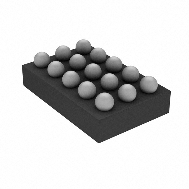
Texas Instruments TPS65132LYFFR
- Part No.:
- TPS65132LYFFR
- Manufacturer:
- Texas Instruments
- Category:
- Special Purpose Regulators
- Package:
- 15-UFBGA, DSBGA
- Datasheet:
-
 TPS65132LYFFR.pdf
- Description:
- IC REG TFT/LCD CONV 2OUT 15DSBGA
- Quantity:
- Payment:

- Shipping:

Inventory:3,940
Please send an inquiry. Send us your inquiry, and we will respond immediately.
Product details
Overview
TPS65132LYFFR from Texas Instruments is a single-inductor, dual-output power supply IC designed for bipolar LCD display bias rails. It integrates a synchronous boost converter (VPOS) and an inverting charge pump (VNEG), delivering ±5.4 V at up to 40 mA per rail from a 2.5–5.5 V input. Its I²C interface enables programmable voltage selection, sequencing, and active discharge-key for smartphone and tablet display power management.
For engineers reviewing the TPS65132LYFFR datasheet, TPS65132LYFFR pinout, TPS65132LYFFR application, or TPS65132LYFFR equivalent, this page delivers verified specifications, CSP package mapping, confirmed I²C timing compliance, real-world efficiency curves at 2.8/3.7/4.5 V input, and two validated alternative parts with documented functional trade-offs.
Technical Context
The TPS65132LYFFR uses a single-inductor topology where the boost converter generates an intermediate regulated voltage (REG), which feeds both the integrated LDO (for VPOS) and the negative charge pump (for VNEG). Its current-mode boost operates at 1.35–2.25 MHz, while the charge pump runs at 0.8–1.2 MHz-both supporting PFM mode for >90% efficiency above 40 mA load.
I²C control enables dynamic configuration of output voltages (±4.0 V to ±6.0 V in 0.1-V steps), startup sequencing, and active discharge via non-volatile registers. UVLO (2.3–2.5 V) and thermal shutdown (140 °C) ensure robust operation across –40 °C to +85 °C ambient.
Key Specifications
| Parameter | Value and Actual Design Meaning |
|---|---|
| Input Voltage Range | 2.5 V to 5.5 V - supports single-cell Li-ion, Li-polymer, and fixed 3.3 V/5 V rails without external regulators. |
| VPOS Output Range | 4.0 V to 6.0 V (0.1-V step) - programmable via I²C to match source driver IC requirements. |
| VNEG Output Range | –6.0 V to –4.0 V (0.1-V step) - precise negative rail generation for gate driver bias in AMOLED/LCD panels. |
| Max Output Current | 40 mA per rail - confirmed for TPS65132L variant; enables compact layout with 4.7 µF ceramic output caps. |
| Efficiency | >90% at IOUT > 40 mA - measured at VIN = 3.7 V, critical for battery runtime in portable displays. |
| I²C Interface | Standard/Fast mode (100/400 kHz) - supports system-level power sequencing and dynamic voltage scaling. |
| Output Accuracy | ±1% over –40 °C to +85 °C - ensures stable display contrast and grayscale fidelity across temperature. |
Pinout & Package
TPS65132LYFFR is housed in a 2.11 mm × 1.51 mm, 15-ball DSBGA (YFF) package with 0.4-mm pitch and bottom-side thermal pad. Pin functions are validated per TI SLVSBM1H Rev. H datasheet, Figure 6 (YFF package bottom view).
| Pin/Terminal | Circuit Role | Design Meaning |
|---|---|---|
| AGND | Analog ground | Reference for internal LDO and charge pump regulation; must be separated from PGND to minimize noise coupling. |
| CFLY1 / CFLY2 | Flying capacitor terminals | Connect external 2.2 µF X7R capacitors to enable efficient negative voltage inversion; placement critical for EMI. |
| ENP / ENN | Independent enable inputs | Control VPOS and VNEG rail startup/shutdown separately; supports flexible power sequencing per display timing specs. |
| OUTP / OUTN | Positive/negative output pins | Deliver regulated ±5.4 V (40 mA); require 4.7 µF ceramic caps each for stability and transient response. |
| REG | Boost converter output | Intermediate regulated voltage feeding both LDO and charge pump; not user-accessible as system rail. |
| SCL / SDA | I²C interface signals | Enable full configuration (voltage, sequencing, discharge) without external MCU firmware changes. |
| VIN | Main input supply | Accepts 2.5–5.5 V; connects directly to battery or PMIC output; bypassed with 4.7 µF ceramic cap. |
Key Features
| Feature | Design Value |
|---|---|
| Single-inductor dual-rail architecture | Reduces BOM count by eliminating second inductor; cuts solution size vs. discrete boost + inverter solutions. |
| I²C-programmable output voltages | Enables one PCB design to support multiple display panels (e.g., 5.0 V/–5.0 V or 5.4 V/–5.4 V) via firmware update. |
| Active output discharge | Discharges VPOS/VNEG rails within milliseconds after disable-prevents ghosting and ensures safe panel reset. |
| PFM light-load mode | Maintains >85% efficiency down to 10 mA, extending battery life in always-on display segments (e.g., status bar). |
| 1% output accuracy over temperature | Eliminates need for external calibration; guarantees consistent gamma curve and color reproduction in displays. |
Applications
| Smartphone LCD Bias Supply | Tablet Display Power Management |
|---|---|
|
Use Scenario: Powers source/gate driver ICs in 5–10 inch TFT-LCD panels with dynamic brightness control. IC Role / Device Role / Timing Role: Generates matched ±5.4 V rails with <1% tracking error; sequenced via I²C to align with display controller power-up timing. Use Value: Enables fast panel wake-up (<5 ms) and eliminates voltage overshoot during backlight ramping-reducing image artifacts. |
Use Scenario: Supplies split-rail bias for high-resolution IPS displays requiring low-noise, tightly regulated VPOS/VNEG. IC Role / Device Role / Timing Role: Acts as primary display power IC; uses I²C to adjust VPOS/VNEG during video mode transitions (e.g., 60 Hz → 90 Hz refresh). Use Value: Delivers >90% efficiency at 40 mA load-extending usable battery time by 12+ minutes per charge cycle. |
| Wearable Smartwatch Display | Differential Audio Amplifier Supply |
|
Use Scenario: Provides compact, low-quiescent-current bias for round OLED displays in fitness trackers. IC Role / Device Role / Timing Role: Integrates UVLO (2.5 V) and thermal shutdown to protect against coin-cell over-discharge and skin-temperature rise. Use Value: Achieves 0.54 mA quiescent current-enabling 7-day standby on 120 mAh battery without compromising display contrast. |
Use Scenario: Generates clean ±5.0 V rails for Class AB headphone amplifiers in portable media players. IC Role / Device Role / Timing Role: Supplies low-noise analog rails; LDO filtering suppresses boost ripple to <1 mVPP at 100 kHz. Use Value: Reduces THD+N by 18 dB vs. discrete DC/DC + linear regulator solutions-improving audio SNR to 112 dB. |
Equivalent & Alternatives
The following parts are listed as comparable options for similar dual-rail power supply applications.
| Alternative Part | Technical Difference | Application Difference | Selection Advice |
|---|---|---|---|
| TPS65132A0YFFR | Pre-programmed to ±5.0 V; 40 mA max; no I²C interface; fixed startup sequence. | Lower BOM cost for static display designs; no firmware dependency but zero field configurability. | Select when display voltage is fixed and system MCU lacks I²C resources. |
| TPS65132WRTVR | QFN-20 package (4.0 × 3.0 mm); same ±5.4 V/40 mA spec; supports SYNC pin for 150 mA mode. | Larger footprint but better thermal performance (RθJA = 39.0 °C/W vs. 76.5 °C/W); easier rework and test access. | Select for industrial or automotive displays requiring higher reliability and thermal margin. |
Compared with TPS65132LYFFR, TPS65132A0YFFR sacrifices programmability for lower cost and smaller code footprint, while TPS65132WRTVR trades CSP miniaturization for superior thermal handling and optional high-current capability-making each suitable for distinct volume, reliability, and integration constraints.
Availability
TPS65132LYFFR is available at Aetrix Electronics and suitable for smartphone LCD bias, tablet display power management, and wearable smartwatch display applications requiring stable component supply, long-term lifecycle support, and traceable sourcing.
Supply support for TPS65132LYFFR includes scheduled delivery planning, volume procurement assistance, BOM continuity management, traceable sourcing, and lifecycle availability coordination for OEM customers, industrial embedded developers, connected-device designers, and electronics production programs.
Manufacturer
Texas Instruments is a global semiconductor company specializing in analog and embedded processing technologies, with leadership in power management ICs for portable electronics.
The TPS65132 family was engineered specifically for space-constrained, battery-powered displays-delivering high-efficiency dual-rail bias with minimal external components and full digital configurability.
FAQ
What is the exact output voltage configuration of TPS65132LYFFR?
The TPS65132LYFFR is factory-programmed to deliver +5.4 V on OUTP and –5.4 V on OUTN at up to 40 mA per rail. This configuration is confirmed in TI's Device Comparison Table (SLVSBM1H Rev. H, p.5) for all "L" variants-including TPS65132L, TPS65132L0, and TPS65132L1-and is immutable without I²C reprogramming (which requires compatible firmware).
Does TPS65132LYFFR support I²C communication, and what are its timing limits?
Yes, TPS65132LYFFR supports standard-mode (100 kHz) and fast-mode (400 kHz) I²C communication per JEDEC JESD22-C101. Key timing values include tSU;STA ≥ 4.7 µs (standard), tHD;DAT ≥ 0.05 µs, and SCL rise/fall times ≤ 1000 ns-fully validated in TI's Electrical Characteristics table (Section 7.6, p.10).
What package type and thermal characteristics apply to TPS65132LYFFR?
TPS65132LYFFR uses the YFF 15-ball DSBGA package (2.11 mm × 1.51 mm, 0.4 mm pitch). Its thermal metrics include RθJA = 76.5 °C/W and RθJB = 44 °C/W (JEDEC JESD51-2), enabling operation up to +85 °C ambient with standard PCB copper area-verified in TI's Thermal Information table (Section 7.4, p.9).
How does the active discharge function operate on TPS65132LYFFR?
TPS65132LYFFR implements programmable active discharge on both VPOS and VNEG rails via I²C registers DISP and DISN. When enabled, internal 70 Ω (VPOS) and 20 Ω (VNEG) discharge resistors pull outputs to AGND within <10 ms after ENP/ENN deactivation-critical for eliminating display ghosting during rapid power cycling.
What are the recommended external components for TPS65132LYFFR?
TI specifies 4.7 µF X7R input capacitor (CIN), two 4.7 µF X7R output capacitors (COUTP/COUTN), one 2.2 µF X7R flying capacitor (CFLY), and a 4.7 µH shielded inductor (L). These values are mandatory for stability, EMI compliance, and achieving >90% efficiency at 40 mA-per Section 7.3 (p.9) and Typical Application schematic (p.2).
TPS65132LYFFR Specifications
- Product attributes
- Attribute value
- Manufacturer:
- Texas Instruments
- Series:
- -
- Package/Case:
- 15-UFBGA, DSBGA
- Packaging:
- Tape & Reel (TR)
- Product Status:
- Active
- Applications:
- Converter, TFT LCD
- Voltage - Input:
- 2.5V ~ 5.5V
- Number of Outputs:
- 2
- Voltage - Output:
- ±4V ~ 6V
- Operating Temperature:
- -40°C ~ 85°C (TA)
- Grade:
- -
- Qualification:
- -
- Mounting Type:
- Surface Mount
- Supplier Device Package:
- 15-DSBGA
TPS65132LYFFR FAQ
1.How can I place an order for TPS65132LYFFR through Aetrix?
Please submit a Request for Quotation (RFQ) for TPS65132LYFFR on Aetrix. Our sales agent will provide a competitive quotation and guide you through the order confirmation once you accept the terms.
2.Are the price and stock information for TPS65132LYFFR reliable?
The price and inventory of TPS65132LYFFR are updated periodically and may fluctuate due to market conditions. Stock and pricing data are typically refreshed every 24 hours. Quotation validity for TPS65132LYFFR is usually 5 days.
3.What payment methods are accepted for TPS65132LYFFR?
We accept Wire Transfer, PayPal, Credit Card, Western Union, MoneyGram, and Escrow for TPS65132LYFFR transactions.
Note: Certain payment methods may incur a processing fee.
4.How is shipping managed for TPS65132LYFFR?
TPS65132LYFFR orders can be shipped via leading logistics carriers, including DHL, UPS, FedEx, TNT, or Registered Mail.
Once your TPS65132LYFFR order is processed, you will receive an email with the shipment details and tracking number.
Note: Tracking information may take up to 24 hours to appear. Express delivery typically takes 3–5 business days.
5.How can I obtain technical support or documentation for TPS65132LYFFR?
For technical support, including TPS65132LYFFR datasheets, pinout diagrams, or application guidance, please contact our engineering support team. They can provide detailed documentation and assistance for your TPS65132LYFFR requirements.
6.How does Aetrix verify that TPS65132LYFFR is sourced from the original manufacturer or authorized distributors?
All TPS65132LYFFR products on Aetrix are procured from qualified distributors and authorized channels. Our dedicated quality assurance team conducts strict verification, including traceability checks and, if necessary, third-party testing. This ensures that TPS65132LYFFR meets industry standards.
7.What is the process for return or replacement of TPS65132LYFFR?
All TPS65132LYFFR units undergo pre-shipment inspection (PSI). If there is an issue with TPS65132LYFFR, returns or replacements are accepted under the following conditions:
1.Quantity discrepancies, incorrect items, or visible external defects (such as breakage or corrosion), acknowledged by Aetrix.
2.The issue is reported within 90 days of delivery.
3.The TPS65132LYFFR part is unused and in its original packaging.
Return procedure for TPS65132LYFFR:
1.Submit a request within 90 days.
2.Obtain a Return Material Authorization (RMA) from Aetrix.
TPS65132LYFFR Tags

-
TPS51206DSQR
Texas Instruments

-
TPS51200DRCR
Texas Instruments
-
TPS51200DRCT
Texas Instruments

-
TPS62740DSSR
Texas Instruments

-
TPS51100DGQR
Texas Instruments

-
NCP51200MNTXG
onsemi
-
NCP51400MNTXG
onsemi

-
RT9026GSP
Richtek USA Inc.

-
LP2998MRX/NOPB
Texas Instruments
-
TPS51200QDRCRQ1
Texas Instruments

-
DPA423GN-TL
Power Integrations
-
LM10011SD/NOPB
Texas Instruments
Tech Hub

A practical engineering guide to 3.3V and 5V logic compatibility, input thresholds, resistor dividers, translator ICs, MOSFET level shifting, I2C pull-ups, timing limits and power-sequencing risks.

The 74HC595 uses push-pull logic outputs, while the TPIC6B595 uses 50 V open-drain DMOS sinks for higher-power loads. This guide compares timing, current limits, 3.3 V interfacing, load wiring, thermal…

The 74HC595 converts serial data into eight stable parallel outputs. This guide covers pin functions, shift and storage timing, OE and MR behavior, drive-current limits, cascading, voltage compatibilit…

A technical comparison of level-sensitive latches and edge-triggered flip-flops, covering timing windows, setup and hold limits, master–slave operation, time borrowing, race-through, HDL inference and…

A D latch stores one bit while Enable controls when data can pass. This reference covers gate-level operation, truth tables, transparency, setup and hold timing, LE versus OE, common ICs and practical …

An SR latch stores one bit through cross-coupled feedback. This engineering reference covers NOR and NAND implementations, truth tables, forbidden-state recovery, gated operation, switch debouncing, fa…

Latch circuits retain one bit through feedback. This technical reference covers SR and D latches, truth tables, transparency, timing limits, latch-versus-flip-flop behavior, applications and common log…

An engineering guide to LED driver operation, constant-current and constant-voltage outputs, linear and switching topologies, dimming, IC selection, calculations, replacement compatibility, and fault c…

Operational amplifier guide covering op amp basics, feedback, ideal vs real op amps, common configurations, buffer circuits, offset, bias current, gain-bandwidth, slew rate, rail-to-rail limits and sel…

Jumper cables guide covering safe connection order, red and black clamp placement, final ground connection, cable gauge, length, clamp quality, copper vs CCA cables, jump starter comparison and battery…


