
 My Inquiry
 My Account


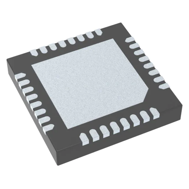
Texas Instruments TPS65680RSNR
- Part No.:
- TPS65680RSNR
- Manufacturer:
- Texas Instruments
- Category:
- Translators, Level Shifters
- Package:
- Datasheet:
-
 TPS65680RSNR.pdf
- Description:
- IC TRANSLTR BIDIRECTIONAL 32QFN
- Quantity:
- Payment:

- Shipping:

Inventory:2,681
Please send an inquiry. Send us your inquiry, and we will respond immediately.
Product details
Overview
TPS65680RSNR from Texas Instruments is a programmable 18-channel LCD panel level shifter IC for GIP/GOA-based displays, delivering 12 high-voltage clock outputs (GCK1–GCK12), 6 high-voltage control outputs (GSP1/GSP2, GCP, GGP1/GGP2, VSS), and integrated overcurrent protection. It operates with VIN = 2.8–5.5 V, VGH = 9–40 V, and VGL1/VGL2 = –4 to –18 V, and supports pattern-programmable timing sequences for TV, monitor, and industrial LCD panels.
For engineers reviewing the TPS65680RSNR datasheet, TPS65680RSNR pinout, TPS65680RSNR application, or TPS65680RSNR equivalent, key selection considerations include its 32-pin WQFN package, I²C-configurable OCP thresholds (20–320 mA), gate-voltage shaping capability, panel discharge sequencing, and dual-VGL support for bipolar LCD biasing.
Technical Context
The TPS65680RSNR implements a user-defined pattern sequencer driven by LN_CLK and LS_START inputs from the timing controller, eliminating need for external frame-synchronized clocks. Its digital core uses an internal 2-MHz oscillator or PLL-synchronized operation (3–15 MHz) with <450 ppm lock accuracy and 8-ms lock time at 40 kHz input.
It integrates independent overcurrent sensing per supply rail (VGH, VGL1, VGL2), with programmable alarm counters (ALARM1 for clock channels, ALARM2 for control channels) and fault recovery requiring full power cycle. Power-good supervision validates all three bias rails before enabling outputs, and panel discharge executes in two configurable steps triggered by LS_CNTRL falling edge.
Key Specifications
| Parameter | Value and Actual Design Meaning |
|---|---|
| VIN Range | 2.8 V to 5.5 V - powers digital core and enables boot from standard logic supply |
| VGH Output Range | 9 V to 40 V - drives high-side gate lines in GOA panels without external boost |
| VGL1/VGL2 Range | –4 V to –18 V - supports bipolar LCD bias with independent negative rails |
| High-Voltage Outputs | 12 clock (GCK1–12) + 6 control (GSP1/2, GCP, GGP1/2, VSS) - fully programmable per-frame timing |
| OCP Threshold | 20 mA to 320 mA in 20-mA steps - configurable per supply rail to match panel capacitance |
| I²C Address | 0x42 (I2CSEL low) or 0x43 (I2CSEL high) - enables dual-device parallel configuration |
| Package | 4.0 mm × 4.0 mm WQFN-32 - thermally enhanced layout with exposed VGL2 pad |
Pinout & Package
The TPS65680RSNR is housed in a 4.0 mm × 4.0 mm, 32-pin WQFN package (RSN) with thermal pad connected to VGL2. Pin functions are validated per TI SLVSE46A datasheet Rev A (January 2018).
| Pin/Terminal | Circuit Role | Design Meaning |
|---|---|---|
| SCL | I²C clock input | Enables register configuration and pattern updates at up to 1 MHz (Fast-mode Plus) |
| SDA | I²C bidirectional data | Supports shared bus with multiple TPS65680RSNR devices via I2CSEL address selection |
| LN_CLK | PLL line-clock input | Reference timing source (40 kHz–500 kHz) for synchronized output sequencing |
| LS_START | Pattern start trigger | Resets internal address pointer to initiate new frame sequence on rising edge |
| GCK1–GCK12 | High-voltage clock outputs | Twelve programmable outputs with charge-sharing/gate-voltage shaping (CS1/CS2 pins) |
| GSP1/GSP2 | Gate start-pulse outputs | Control signals for GOA stage activation; default to VGL2 when inactive |
| VSS | Switched low-side supply | Provides active discharge path tied to VGL2; used in panel shutdown sequencing |
Key Features
| Feature | Design Value |
|---|---|
| Programmable output pattern | On-chip nonvolatile memory stores default timing sequences-enables one PCB to drive multiple LCD panels without hardware change |
| 2-wire TCON interface | Reduces TCON I/O count and simplifies routing: only LN_CLK and LS_START required for full frame control |
| Gate-voltage shaping & charge-sharing | CS1/CS2 pins enable waveform optimization for reduced EMI and improved gate driver efficiency in high-resolution panels |
| Panel discharge sequencing | Two-step, register-configurable shutdown (DISCHARGE STEP1/STEP2) prevents latch-up and extends panel lifetime |
| Per-rail overcurrent protection | Detects faults on VGH, VGL1, and VGL2 independently; triggers HiZ output state and FAULT mode with alarm counters |
Applications
| TV Display Panels | Industrial HMI Displays |
|---|---|
Use Scenario: Large-format LCD TVs using GOA (Gate-Only-Array) architecture with integrated gate drivers. IC Role / Device Role / Timing Role: TPS65680RSNR generates all 12 clock phases and 6 control signals (GSP, GCP, VSS) to drive row-by-row gate activation and panel discharge. Use Value: Eliminates need for discrete level shifters and reduces BOM count; programmable patterns accommodate panel revisions without PCB re-spin. | Use Scenario: Ruggedized industrial monitors deployed in factory automation systems requiring long-term display reliability. IC Role / Device Role / Timing Role: TPS65680RSNR provides fault-resilient bias sequencing with overcurrent detection on VGH/VGL rails and controlled panel discharge during power loss. Use Value: Prevents gate oxide damage during brownout events; thermal shutdown (130°C) and UVLO ensure safe operation in uncontrolled environments. |
| Notebook/Tablet LCDs | Public Signage Panels |
Use Scenario: High-DPI notebook and tablet displays using GIP (Gate-In-Panel) technology with tight timing margins. IC Role / Device Role / Timing Role: TPS65680RSNR delivers sub-200 ns propagation delay (GCK rising/falling) and precise inter-channel timing (255 SEQ_CLK cycles between GCKs). Use Value: Meets strict setup/hold requirements of fast-refresh panels; I²C reconfiguration supports late-stage panel tuning during design validation. | Use Scenario: Outdoor digital signage with wide temperature range (-40°C to +85°C ambient) and high-brightness backlighting. IC Role / Device Role / Timing Role: TPS65680RSNR manages dual-negative supplies (VGL1/VGL2) for stable contrast across temperature and enables VGH discharge during scheduled shutdown. Use Value: Maintains consistent grayscale performance; programmable EN_DLY timer ensures reliable startup after cold boot. |
Equivalent & Alternatives
The following parts are listed as comparable options for similar LCD panel level shifter applications.
| Alternative Part | Technical Difference | Application Difference | Selection Advice |
|---|---|---|---|
| TPS65682RSNR | Same 32-pin WQFN package and pinout; adds integrated VCOM amplifier and VDDIO regulator not present in TPS65680RSNR | Targeted at panels requiring analog VCOM correction and I/O voltage regulation; higher BOM cost and complexity | Select TPS65682RSNR only if VCOM buffering or regulated I/O supply is required; otherwise TPS65680RSNR offers lower cost and simpler biasing |
| BD8153FVJ-E2 | 12-channel clock + 4-control-output level shifter; no CS1/CS2 charge-sharing, no panel discharge sequencing, no VGL2 pad | Designed for smaller panels (≤15") with fixed timing; lacks programmability and dual-VGL support | BD8153FVJ-E2 suits cost-sensitive, low-channel-count designs where pattern flexibility and bipolar biasing are unnecessary |
Compared with TPS65680RSNR, TPS65682RSNR adds analog VCOM support but increases system complexity, while BD8153FVJ-E2 reduces channel count and eliminates programmability-making TPS65680RSNR optimal for mid-to-large GOA panels needing field-tunable timing and robust dual-rail discharge.
Availability
TPS65680RSNR is available at Aetrix Electronics and suitable for TV display modules, industrial HMI systems, and notebook LCD biasing requiring stable component supply, long-lifecycle availability, and automotive-grade reliability screening.
Supply support for TPS65680RSNR includes scheduled delivery planning, volume procurement assistance, BOM continuity management, traceable sourcing, and lifecycle availability coordination for OEM customers, industrial embedded developers, connected-device designers, and electronics production programs.
Manufacturer
Texas Instruments is a global semiconductor leader specializing in analog, embedded processing, and power management technologies, with decades of experience in display interface and bias solutions.
The TPS65680RSNR belongs to TI's LCD panel power and timing IC product line, engineered specifically for GOA/GIP architectures to replace discrete level-shifting and sequencing circuits in large-format, high-resolution displays.
FAQ
What is the primary function of the TPS65680RSNR in an LCD system?
The TPS65680RSNR serves as a programmable high-voltage level shifter that generates all timing signals for GOA/GIP LCD panels-including 12 clock outputs (GCK1–GCK12), 6 control outputs (GSP1/GSP2, GCP, GGP1/GGP2, VSS), and panel discharge sequencing. It replaces multiple discrete level shifters and simplifies timing controller (TCON) interface with only two required signals: LN_CLK and LS_START. The TPS65680RSNR enables flexible, software-defined panel driving without hardware changes.
How does the TPS65680RSNR handle overcurrent protection?
The TPS65680RSNR implements per-rail overcurrent protection (OCP) on VGH, VGL1, and VGL2 supplies, with thresholds adjustable from 20 mA to 320 mA in 20-mA steps via I²C registers. It maintains separate alarm counters (ALARM1 for clock channels, ALARM2 for control channels); exceeding the programmed event limit forces all outputs into HiZ and enters FAULT mode. Recovery requires a full power cycle-no automatic reset. This behavior is documented in the TPS65680RSNR datasheet Section 7.3.5 and electrical characteristics Table 6.5.
Can the TPS65680RSNR support dual-negative bias supplies (VGL1 and VGL2)?
Yes, the TPS65680RSNR explicitly supports independent VGL1 and VGL2 supplies ranging from –4 V to –18 V each. VGL1 powers GCK7/GCK8 outputs, while VGL2 connects to the thermal pad and supplies GCK1–GCK6, GCK9–GCK12, GSP1/GSP2, GCP, GGP1/GGP2, and VSS. If only one negative supply is available, VGL1 and VGL2 must be shorted together per datasheet Section 7.3.1. The thermal pad must be connected to the most negative supply-either dedicated VGL2 or VGL1 if shared.
What is the role of the CS1 and CS2 pins on the TPS65680RSNR?
CS1 and CS2 are charge-sharing and gate-voltage shaping terminals on the TPS65680RSNR. CS1 connects to GCK1–GCK6 outputs to shape their waveforms and reduce ringing; CS2 connects to GCK7–GCK12 for the same purpose. These pins allow external RC networks to fine-tune rise/fall times and overshoot, improving EMI performance and gate driver efficiency in high-resolution LCD panels. Their use is optional-pins may be left floating if not needed-and is detailed in the TPS65680RSNR pin function table (Section 5) and feature description (Section 7.3.7).
Does the TPS65680RSNR require external programming during normal operation?
No-the TPS65680RSNR stores default configuration and pattern data in on-chip nonvolatile memory (NVM), allowing it to boot and operate autonomously after power-up without external programming. I²C writes are optional and used only for dynamic updates (e.g., panel tuning, firmware patches). NVM supports up to 9 write cycles with 10-year data retention at TJ ≤85°C. The TPS65680RSNR datasheet specifies boot time as 1.5 ms from VIN crossing UVLO to readiness for I²C communication, confirming self-contained startup behavior.
TPS65680RSNR Specifications
- Product attributes
- Attribute value
- Manufacturer:
- Texas Instruments
- Series:
- -
- Package/Case:
- Packaging:
- Tape & Reel (TR)
- Product Status:
- Active
- Translator Type:
- Voltage Level
- Channel Type:
- Bidirectional
- Number of Circuits:
- 1
- Channels per Circuit:
- 18
- Voltage - VCCA:
- -
- Voltage - VCCB:
- -
- Input Signal:
- -
- Output Signal:
- -
- Output Type:
- Programmable
- Data Rate:
- -
- Operating Temperature:
- -40°C ~ 85°C (TJ)
- Grade:
- -
- Qualification:
- -
- Features:
- -
- Mounting Type:
- Surface Mount
- Supplier Device Package:
- 32-WFQFN Exposed Pad
TPS65680RSNR FAQ
1.How can I place an order for TPS65680RSNR through Aetrix?
Please submit a Request for Quotation (RFQ) for TPS65680RSNR on Aetrix. Our sales agent will provide a competitive quotation and guide you through the order confirmation once you accept the terms.
2.Are the price and stock information for TPS65680RSNR reliable?
The price and inventory of TPS65680RSNR are updated periodically and may fluctuate due to market conditions. Stock and pricing data are typically refreshed every 24 hours. Quotation validity for TPS65680RSNR is usually 5 days.
3.What payment methods are accepted for TPS65680RSNR?
We accept Wire Transfer, PayPal, Credit Card, Western Union, MoneyGram, and Escrow for TPS65680RSNR transactions.
Note: Certain payment methods may incur a processing fee.
4.How is shipping managed for TPS65680RSNR?
TPS65680RSNR orders can be shipped via leading logistics carriers, including DHL, UPS, FedEx, TNT, or Registered Mail.
Once your TPS65680RSNR order is processed, you will receive an email with the shipment details and tracking number.
Note: Tracking information may take up to 24 hours to appear. Express delivery typically takes 3–5 business days.
5.How can I obtain technical support or documentation for TPS65680RSNR?
For technical support, including TPS65680RSNR datasheets, pinout diagrams, or application guidance, please contact our engineering support team. They can provide detailed documentation and assistance for your TPS65680RSNR requirements.
6.How does Aetrix verify that TPS65680RSNR is sourced from the original manufacturer or authorized distributors?
All TPS65680RSNR products on Aetrix are procured from qualified distributors and authorized channels. Our dedicated quality assurance team conducts strict verification, including traceability checks and, if necessary, third-party testing. This ensures that TPS65680RSNR meets industry standards.
7.What is the process for return or replacement of TPS65680RSNR?
All TPS65680RSNR units undergo pre-shipment inspection (PSI). If there is an issue with TPS65680RSNR, returns or replacements are accepted under the following conditions:
1.Quantity discrepancies, incorrect items, or visible external defects (such as breakage or corrosion), acknowledged by Aetrix.
2.The issue is reported within 90 days of delivery.
3.The TPS65680RSNR part is unused and in its original packaging.
Return procedure for TPS65680RSNR:
1.Submit a request within 90 days.
2.Obtain a Return Material Authorization (RMA) from Aetrix.
TPS65680RSNR Tags
-
74LVC1T45GW,125
Nexperia USA Inc.
-
74LVCH2T45DC,125
Nexperia USA Inc.

-
SN74LVC1T45DBVR
Texas Instruments
-
SN74LVC1T45DRLR
Texas Instruments
-
SN74LVC1T45DPKR
Texas Instruments
-
SN74LVC2T45DCTR
Texas Instruments
-
74LVC2T45GT,115
Nexperia USA Inc.
-
SN74LVC1T45YZPR
Texas Instruments

-
LSF0102DCUR
Texas Instruments

-
SN74LVC1T45DCKR
Texas Instruments
-
TXS0102DCTR
Texas Instruments
-
FXLP34P5X
onsemi
Tech Hub

A practical engineering guide to 3.3V and 5V logic compatibility, input thresholds, resistor dividers, translator ICs, MOSFET level shifting, I2C pull-ups, timing limits and power-sequencing risks.

The 74HC595 uses push-pull logic outputs, while the TPIC6B595 uses 50 V open-drain DMOS sinks for higher-power loads. This guide compares timing, current limits, 3.3 V interfacing, load wiring, thermal…

The 74HC595 converts serial data into eight stable parallel outputs. This guide covers pin functions, shift and storage timing, OE and MR behavior, drive-current limits, cascading, voltage compatibilit…

A technical comparison of level-sensitive latches and edge-triggered flip-flops, covering timing windows, setup and hold limits, master–slave operation, time borrowing, race-through, HDL inference and…

A D latch stores one bit while Enable controls when data can pass. This reference covers gate-level operation, truth tables, transparency, setup and hold timing, LE versus OE, common ICs and practical …

An SR latch stores one bit through cross-coupled feedback. This engineering reference covers NOR and NAND implementations, truth tables, forbidden-state recovery, gated operation, switch debouncing, fa…

Latch circuits retain one bit through feedback. This technical reference covers SR and D latches, truth tables, transparency, timing limits, latch-versus-flip-flop behavior, applications and common log…

An engineering guide to LED driver operation, constant-current and constant-voltage outputs, linear and switching topologies, dimming, IC selection, calculations, replacement compatibility, and fault c…

Operational amplifier guide covering op amp basics, feedback, ideal vs real op amps, common configurations, buffer circuits, offset, bias current, gain-bandwidth, slew rate, rail-to-rail limits and sel…

Jumper cables guide covering safe connection order, red and black clamp placement, final ground connection, cable gauge, length, clamp quality, copper vs CCA cables, jump starter comparison and battery…


