
 My Inquiry
 My Account


Texas Instruments TPS68470YFFR
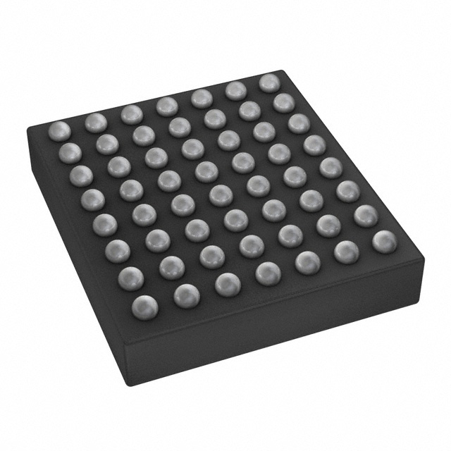
- Part No.:
- TPS68470YFFR
- Manufacturer:
- Texas Instruments
- Category:
- LED Drivers
- Package:
- 56-UFBGA, DSBGA
- Datasheet:
-
 TPS68470YFFR.pdf
- Description:
- IC LED DRIVER RGLTR 1A 56DSBGA
- Quantity:
- Payment:

- Shipping:

Inventory:1,426
Please send an inquiry. Send us your inquiry, and we will respond immediately.
Product details
Overview
TPS68470YFFR from Texas Instruments is a highly integrated power management unit (PMU) designed specifically for compact camera modules (CCMs), combining a 500-mA buck converter, dual 1-A flash LED drivers with temperature monitoring and open/short detection, five programmable LDOs (including VCM, analog, IO, sensor IO, and auxiliary rails), and a PLL-based clock generator with crystal oscillator support. It powers world-facing and user-facing cameras in smartphones and tablets while delivering reference clocks to image sensors.
For engineers reviewing the TPS68470YFFR datasheet, TPS68470YFFR pinout, TPS68470YFFR application, or TPS68470YFFR equivalent, this device is evaluated for CCM power rail consolidation, flash timing control, sensor clock synchronization, thermal-aware LED current regulation, and I²C-configurable multi-rail sequencing in space-constrained mobile imaging systems.
Technical Context
The TPS68470YFFR integrates a synchronous buck converter (3–6 MHz switching frequency, 0.9–1.95 V output) for digital core supply and a high-efficiency boost converter (5.5 V max output, 4 A switch current limit) driving two low-side 1-A LED current sinks with adaptive voltage regulation based on LED forward voltage. Its clock subsystem includes a 3–27 MHz crystal oscillator and a programmable PLL generating HCLK_A/HCLK_B outputs (3.8–64.2 MHz) with <600 ps cycle-to-cycle jitter.
Five independent LDOs-LDO_ANA (200 mA, 0.875–3.1 V), LDO_VCM (500 mA, 0.875–3.1 V), LDO_IO (50 mA, ≥1.6 V min), LDO_S_IO (150 mA, 0.875–3.1 V), and LDO_AUX1/AUX2 (150/80 mA, 0.875–3.1 V)-are digitally programmable via I²C using 17.8-mV steps and feature short-circuit protection, thermal shutdown (140–160 °C trip), and controlled ramp-up/down. All rails support dynamic voltage scaling and independent enable/disable control.
Key Specifications
| Parameter | Value and Actual Design Meaning |
|---|---|
| Buck Output Current | 500 mA max - powers image sensor digital core with fast 85–200 µs ramp-up time and internal discharge resistor for clean power-down sequencing. |
| Flash LED Drivers | Dual 1-A low-side current sinks - supports simultaneous or staggered flash operation with NTC-based temperature compensation and open/short fault detection. |
| LDO_ANA Output | 0.875–3.1 V @ 200 mA - supplies image sensor analog circuitry with ±2% DC accuracy, 100–150 mV dropout, and 56 dB PSRR at 1 kHz. |
| HCLK Clock Range | 3.8–64.2 MHz - programmable sensor clock output with 45–55% duty cycle, <5 ns rise/fall time, and ≤600 ps cycle-to-cycle jitter for precise timing alignment. |
| I²C Interface | Standard/fast-mode (400 kHz), 3.3-V tolerant - enables full configuration of all regulators, clock dividers, GPIOs, and fault reporting registers. |
| Package | 56-pin DSBGA (YFF), 3.325 mm × 2.930 mm, 0.625 mm height - optimized for ultra-thin mobile camera module PCB stacking with minimal footprint. |
| Operating Temp | 0°C to +85°C ambient - validated for smartphone and tablet CCM use cases with thermal shutdown on buck, boost, and LDO sections. |
Pinout & Package
TPS68470YFFR uses a 56-pin DSBGA (YFF) package measuring 3.325 mm × 2.930 mm with 0.625 mm profile, designed for high-density camera module integration. Pin functions are defined per TI SLVSCJ1B datasheet Rev B (Jan 2017).
| Pin/Terminal | Circuit Role | Design Meaning |
|---|---|---|
| WLED_SW / WLED_OUT / WLED_GND | Boost converter power stage | Three dedicated pins per node (SW: F3/F2/F1; OUT: E3/E2/E1; GND: G3/G2/G1) reduce parasitic inductance for stable 5.5-V boost output and efficient 1-A LED drive. |
| DRV_WLED1 / DRV_WLED2 | LED current sink terminals | Low-side current sources (H1, H3) sink up to 1 A each from WLED_OUT; sense voltage fixed at 400 mV for accurate current regulation. |
| HCLK_A / HCLK_B | Sensor clock outputs | Dual programmable clock outputs (D5, C5) drive image sensor pixel clocks with matched timing and configurable drive strength (2/4/6/8 mA). |
| ANA_OUT / VCM_OUT / IO_OUT / S_IO_OUT / AUX1_OUT / AUX2_OUT | LDO regulated outputs | Six independent LDO outputs with separate enable/control; ANA_OUT (B7) and VCM_OUT (H4) support highest current (200/500 mA) and lowest noise requirements. |
| I2C_ICA / I2C_ICB / SDA / SCL | I²C address and bus interface | Hardware address pins (G4, F4) set device address; SDA (F5) and SCL (G5) support standard/fast-mode communication with 3.3-V tolerance. |
| GPIO0–GPIO6 | Configurable general-purpose I/O | Seven bidirectional pins (D3, D6, F6, C3, C4, C6, E6) usable as sensor SDA/SCL daisy-chain interfaces, external clock inputs, or system control signals. |
Key Features
| Feature | Design Value |
|---|---|
| Adaptive Flash Boost Regulation | Automatically adjusts WLED_OUT voltage to match LED forward voltage, minimizing power loss and heat generation during flash operation. |
| Integrated Sensor Clock Generation | Eliminates need for external clock IC by providing two synchronized, jitter-controlled HCLK outputs (3.8–64.2 MHz) directly from PLL + crystal oscillator. |
| Thermal-Aware LED Control | Monitors LED temperature via WLED_NTC (C2) using 23.8-µA bias current and triggers warning/hot flags at defined thermistor resistance thresholds. |
| Multi-Rail Programmable LDOs | Five LDOs (ANA, VCM, IO, S_IO, AUX1/AUX2) independently configurable from 0.875 V to 3.1 V in 17.8-mV steps via I²C, enabling optimal voltage scaling per subsystem. |
| Comprehensive Fault Protection | Includes open/short LED detection, thermal shutdown (140–160 °C), output short detection (0.5 V threshold), and UVLO on both 3V3_VDD and 3V3_SUS inputs. |
Applications
| Smartphone Front/Rear Camera Module | Tablet Integrated Imaging System |
|---|---|
|
Use Scenario: Powers dual-camera CCMs in slim-profile smartphones requiring simultaneous flash, sensor clocking, and analog/digital rail separation. IC Role / Device Role / Timing Role: PMU provides CORE (buck), ANA (LDO_ANA), VCM (LDO_VCM), and flash (boost + drivers); generates HCLK_A/B for sensor timing sync. Use Value: Reduces BOM count by consolidating 7 power rails + clock + flash into single YFF package, enabling <3.5-mm module thickness. |
Use Scenario: Supplies imaging subsystem in detachable ultrabooks and tablets where thermal headroom and layout area are constrained. IC Role / Device Role / Timing Role: Delivers regulated IO, S_IO, and AUX rails to companion processors and sensors; uses GPIO daisy-chaining to extend I²C to secondary sensors. Use Value: Enables flexible rail sequencing and dynamic voltage scaling across multiple sensors without external sequencers or discrete regulators. |
| Compact Camera Module Reference Design | Mobile AR/VR Depth Sensing Module |
|
Use Scenario: Used in TI's CCM reference designs to demonstrate full power, clock, and flash integration for 13-MP+ image sensors. IC Role / Device Role / Timing Role: Acts as central PMU with I²C register map controlling all voltages, clocks, LED strobes, and fault responses in one firmware interface. Use Value: Accelerates design-in with pre-validated layout, thermal performance, and timing margins-reducing qualification time by ≥4 weeks. |
Use Scenario: Powers time-of-flight (ToF) or structured-light depth sensors requiring precise flash timing, low-noise analog rails, and synchronized clocks. IC Role / Device Role / Timing Role: Generates jitter-controlled HCLK for sensor exposure timing; regulates low-noise ANA_OUT for ToF analog front-end; drives flash LEDs with microsecond-level strobe control. Use Value: Achieves sub-1% depth measurement error by eliminating clock skew between illumination and capture timing domains. |
Equivalent & Alternatives
The following parts are listed as comparable options for similar power management and LED driver applications.
| Alternative Part | Technical Difference | Application Difference | Selection Advice |
|---|---|---|---|
| TPS68480YFFR | Successor with enhanced thermal performance, higher LDO_VCM current (600 mA), and extended HCLK range (up to 128 MHz); same pinout and register compatibility. | Targets next-gen high-resolution CCMs requiring faster sensor clocks and higher VCM drive for larger actuators. | Select when upgrading for >64-MHz sensor clocks or >500-mA VCM loads; retains software and layout compatibility. |
| MAX20049ATPA/VY+ | Dual 1.2-A flash drivers, 40-V input capability, integrated I²C watchdog; lacks integrated clock generator and has only three LDOs. | Used in automotive ADAS cameras where input voltage transients exceed 3.63 V and functional safety monitoring is required. | Choose for 4.5–40-V input environments or ASIL-B systems; requires external clock source and additional LDOs for full CCM support. |
Compared with TPS68470YFFR, TPS68480YFFR offers higher clock frequency and VCM current in identical packaging, while MAX20049ATPA/VY+ trades clock integration for wider VIN and safety features-making TPS68470YFFR optimal for cost-sensitive, space-constrained mobile CCMs needing full clock+power+flash integration.
Availability
TPS68470YFFR is available at Aetrix Electronics and suitable for smartphone camera modules, tablet imaging subsystems, and compact camera module reference designs requiring stable component supply, long-term lifecycle support, and traceable sourcing for production ramp.
Supply support for TPS68470YFFR includes scheduled delivery planning, volume procurement assistance, BOM continuity management, traceable sourcing, and lifecycle availability coordination for OEM customers, industrial embedded developers, connected-device designers, and electronics production programs.
Manufacturer
Texas Instruments is a global semiconductor leader specializing in analog, embedded processing, and power management technologies, with decades of experience in mobile and imaging power solutions.
The TPS68470YFFR belongs to TI's Compact Camera Module PMU product line, engineered to consolidate power, clock, and flash functions into a single ultra-thin package for space-constrained mobile imaging applications.
FAQ
What is the maximum output current capability of the TPS68470YFFR buck converter?
The TPS68470YFFR buck converter delivers up to 500 mA continuous output current to the image sensor digital core. It features a 180-mΩ high-side and 150-mΩ low-side MOSFET, 3–6 MHz switching frequency, and internal discharge resistor (190–375 Ω) for controlled power-down sequencing. This rating is validated across 0°C to 85°C ambient with proper thermal layout per TI SLVSCJ1B.
How does the TPS68470YFFR support LED temperature monitoring for flash safety?
The TPS68470YFFR monitors LED temperature via the WLED_NTC pin (C2), which sources a precise 23.8-µA bias current into an external NTC thermistor. The device compares resulting voltage against two thresholds: 0.92–1.19 V (LEDWARN flag) and 0.29–0.40 V (LEDHOT flag), enabling firmware to throttle or disable flash before thermal damage occurs. This function operates independently of I²C control.
Can the TPS68470YFFR generate clocks for two different image sensors simultaneously?
Yes, the TPS68470YFFR provides two independent, programmable clock outputs-HCLK_A (D5) and HCLK_B (C5)-each configurable from 3.8 MHz to 64.2 MHz with <600 ps cycle-to-cycle jitter. Both outputs derive from the same PLL but support separate post-dividers and drive strengths, allowing asynchronous or phase-aligned timing for dual-sensor systems such as stereo or time-of-flight configurations.
What are the minimum and maximum output voltage ranges for the LDOs in the TPS68470YFFR?
All five LDOs in the TPS68470YFFR (LDO_ANA, LDO_VCM, LDO_IO, LDO_S_IO, LDO_AUX1/AUX2) are programmable from 0.875 V to 3.1 V in precise 17.8-mV steps via I²C voltage adjustment registers. LDO_IO has a hard minimum of 1.6 V to ensure I²C functionality, while LDO_VCM supports up to 500 mA load current at any setting within the range.
Does the TPS68470YFFR support daisy-chained I²C communication with image sensors?
Yes, the TPS68470YFFR supports I²C daisy-chaining through GPIO1 (D6) and GPIO2 (F6), which can be configured as sensor SDA and SCL pass-gates with 25-Ω on-resistance. This allows the host processor to access downstream sensors over a shared I²C bus without additional level shifters or multiplexers, reducing interconnect complexity in multi-sensor modules.
TPS68470YFFR Specifications
- Product attributes
- Attribute value
- Manufacturer:
- Texas Instruments
- Series:
- -
- Package/Case:
- 56-UFBGA, DSBGA
- Packaging:
- Tape & Reel (TR)
- Product Status:
- Active
- Type:
- DC DC Regulator
- Topology:
- Step-Down (Buck), Step-Up (Boost)
- Internal Switch(s):
- Yes
- Number of Outputs:
- 3
- Voltage - Supply (Min):
- 2.97V
- Voltage - Supply (Max):
- 3.63V
- Voltage - Output:
- -
- Current - Output / Channel:
- 1A (Flash)
- Frequency:
- -
- Dimming:
- -
- Applications:
- Camera Flash
- Operating Temperature:
- 0°C ~ 85°C (TA)
- Grade:
- -
- Qualification:
- -
- Mounting Type:
- Surface Mount
- Supplier Device Package:
- 56-DSBGA (3.33x2.93)
TPS68470YFFR FAQ
1.How can I place an order for TPS68470YFFR through Aetrix?
Please submit a Request for Quotation (RFQ) for TPS68470YFFR on Aetrix. Our sales agent will provide a competitive quotation and guide you through the order confirmation once you accept the terms.
2.Are the price and stock information for TPS68470YFFR reliable?
The price and inventory of TPS68470YFFR are updated periodically and may fluctuate due to market conditions. Stock and pricing data are typically refreshed every 24 hours. Quotation validity for TPS68470YFFR is usually 5 days.
3.What payment methods are accepted for TPS68470YFFR?
We accept Wire Transfer, PayPal, Credit Card, Western Union, MoneyGram, and Escrow for TPS68470YFFR transactions.
Note: Certain payment methods may incur a processing fee.
4.How is shipping managed for TPS68470YFFR?
TPS68470YFFR orders can be shipped via leading logistics carriers, including DHL, UPS, FedEx, TNT, or Registered Mail.
Once your TPS68470YFFR order is processed, you will receive an email with the shipment details and tracking number.
Note: Tracking information may take up to 24 hours to appear. Express delivery typically takes 3–5 business days.
5.How can I obtain technical support or documentation for TPS68470YFFR?
For technical support, including TPS68470YFFR datasheets, pinout diagrams, or application guidance, please contact our engineering support team. They can provide detailed documentation and assistance for your TPS68470YFFR requirements.
6.How does Aetrix verify that TPS68470YFFR is sourced from the original manufacturer or authorized distributors?
All TPS68470YFFR products on Aetrix are procured from qualified distributors and authorized channels. Our dedicated quality assurance team conducts strict verification, including traceability checks and, if necessary, third-party testing. This ensures that TPS68470YFFR meets industry standards.
7.What is the process for return or replacement of TPS68470YFFR?
All TPS68470YFFR units undergo pre-shipment inspection (PSI). If there is an issue with TPS68470YFFR, returns or replacements are accepted under the following conditions:
1.Quantity discrepancies, incorrect items, or visible external defects (such as breakage or corrosion), acknowledged by Aetrix.
2.The issue is reported within 90 days of delivery.
3.The TPS68470YFFR part is unused and in its original packaging.
Return procedure for TPS68470YFFR:
1.Submit a request within 90 days.
2.Obtain a Return Material Authorization (RMA) from Aetrix.
TPS68470YFFR Tags

-
BCR402RE6327HTSA1
Infineon Technologies

-
BCR430UXTSA2
Infineon Technologies

-
BCR420UE6433HTMA1
Infineon Technologies
-
BCR420UE6327HTSA1
Infineon Technologies
-
BCR421UE6327HTSA1
Infineon Technologies

-
LYT1604D-TL
Power Integrations

-
HV9910CLG-G
Microchip Technology

-
CL2N8-G
Microchip Technology

-
BCR420UW6-7
Diodes Incorporated
-
BCR421UW6-7
Diodes Incorporated

-
BCR420UFD-7
Diodes Incorporated
-
BCR421UFD-7
Diodes Incorporated
Tech Hub

A practical engineering guide to 3.3V and 5V logic compatibility, input thresholds, resistor dividers, translator ICs, MOSFET level shifting, I2C pull-ups, timing limits and power-sequencing risks.

The 74HC595 uses push-pull logic outputs, while the TPIC6B595 uses 50 V open-drain DMOS sinks for higher-power loads. This guide compares timing, current limits, 3.3 V interfacing, load wiring, thermal…

The 74HC595 converts serial data into eight stable parallel outputs. This guide covers pin functions, shift and storage timing, OE and MR behavior, drive-current limits, cascading, voltage compatibilit…

A technical comparison of level-sensitive latches and edge-triggered flip-flops, covering timing windows, setup and hold limits, master–slave operation, time borrowing, race-through, HDL inference and…

A D latch stores one bit while Enable controls when data can pass. This reference covers gate-level operation, truth tables, transparency, setup and hold timing, LE versus OE, common ICs and practical …

An SR latch stores one bit through cross-coupled feedback. This engineering reference covers NOR and NAND implementations, truth tables, forbidden-state recovery, gated operation, switch debouncing, fa…

Latch circuits retain one bit through feedback. This technical reference covers SR and D latches, truth tables, transparency, timing limits, latch-versus-flip-flop behavior, applications and common log…

An engineering guide to LED driver operation, constant-current and constant-voltage outputs, linear and switching topologies, dimming, IC selection, calculations, replacement compatibility, and fault c…

Operational amplifier guide covering op amp basics, feedback, ideal vs real op amps, common configurations, buffer circuits, offset, bias current, gain-bandwidth, slew rate, rail-to-rail limits and sel…

Jumper cables guide covering safe connection order, red and black clamp placement, final ground connection, cable gauge, length, clamp quality, copper vs CCA cables, jump starter comparison and battery…


