
 My Inquiry
 My Account


Texas Instruments TPS7A6033QKVURQ1
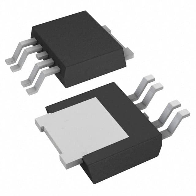
- Part No.:
- TPS7A6033QKVURQ1
- Manufacturer:
- Texas Instruments
- Package:
- TO-252-5, DPAK (4 Leads + Tab), TO-252AD
- Datasheet:
-
 TPS7A6033QKVURQ1.pdf
- Description:
- IC REG LINEAR 3.3V 300MA TO252-5
- Quantity:
- Payment:

- Shipping:

Inventory:2,961
Please send an inquiry. Send us your inquiry, and we will respond immediately.
Product details
Overview
TPS7A6033QKVURQ1 from Texas Instruments is an AEC-Q100 Grade 1 automotive-grade LDO regulator delivering fixed 3.3 V output at up to 300 mA, with 25 µA typical quiescent current, 7–40 V input range, and integrated programmable power-on-reset functionality. It operates in automotive head units and instrument clusters where low standby power and transient resilience are critical.
For engineers reviewing the TPS7A6033QKVURQ1 datasheet, TPS7A6033QKVURQ1 pinout, TPS7A6033QKVURQ1 application, or TPS7A6033QKVURQ1 equivalent, this device supports cold-crank operation via low-voltage tracking, enables robust system initialization with capacitor-programmable reset delay (100 pF–100 nF), and provides fault protection including thermal shutdown and short-circuit current limiting.
Technical Context
The TPS7A6033QKVURQ1 implements a monolithic PMOS pass transistor architecture with internal charge-pump biasing for stable regulation across its 7–40 V input range. Its programmable reset delay uses an external capacitor on the RDELAY pin to set tPOR from 300 µs (100 pF) to 300 ms (100 nF), while the open-drain nRST output asserts after delay completion when VOUT exceeds 93% of 3.3 V.
It integrates undervoltage lockout (VIN-UVLO = 3.16 V), thermal shutdown (TSHUTDOWN = 165 °C, THYST = 10 °C), and overcurrent protection (ICL = 350–1000 mA). The device enters ultra-low-power sleep mode (<2 µA) only when disabled - but TPS7A6033QKVURQ1 lacks an ENABLE pin and is always active upon valid VIN.
Key Specifications
| Parameter | Value and Actual Design Meaning |
|---|---|
| Output Voltage | Fixed 3.3 V ±2% over load (10–300 mA), line (7–28 V), and temperature (–40°C to 150°C) |
| Input Voltage Range | 7 V to 40 V continuous; withstands 45-V transients for <480 ms per absolute rating |
| Quiescent Current | 25 µA typical at light load (0.01–0.75 mA); drops to <2 µA only if externally disabled (not applicable - no ENABLE) |
| Dropout Voltage | 300 mV at 150 mA load; 500 mV at 250 mA - defines minimum VIN needed for regulation |
| Reset Delay Range | Programmable via CDLY: 300 µs (100 pF) to 300 ms (100 nF); internally fixed at 250 µs if CDLY unconnected |
| PSRR | 60 dB at 100 Hz / 300 mA; 30 dB at 150 kHz / 300 mA - critical for noise-sensitive MCU power rails |
| Thermal Protection | Thermal shutdown at 165 °C with 10 °C hysteresis; RθJA = 26.9 °C/W (TO-252 package) |
Pinout & Package
TPS7A6033QKVURQ1 is packaged in a 5-pin TO-252 (KVU/DPAK) with exposed thermal pad, measuring 6.10 mm × 6.60 mm. The package supports high-power dissipation in automotive under-hood environments and requires soldering the thermal pad to a PCB copper pour for optimal thermal performance.
| Pin/Terminal | Circuit Role | Design Meaning |
|---|---|---|
| VIN | Unregulated input supply | Accepts 7–40 V; must be bypassed with CIN to GND to suppress transients; tolerates 45-V spikes |
| nRST | Open-drain reset output | Asserts low during power-up until VOUT reaches 93% of 3.3 V and tPOR elapses; requires external pullup to VOUT |
| GND | Signal and power ground reference | Common return path for VIN, VOUT, and internal circuitry; connects to thermal pad for heat sinking |
| RDELAY | Reset delay timing capacitor node | Connects external CDLY (100 pF–100 nF) to GND to program tPOR; charges at 1 µA typical to 3.3 V threshold |
| VOUT | Regulated 3.3 V output | Delivers up to 300 mA; requires low-ESR ceramic COUT (≥10 µF) for stability; tracks VIN below dropout |
Key Features
| Feature | Design Value |
|---|---|
| Programmable Power-On Reset | Capacitor-timed delay (300 µs–300 ms) ensures reliable MCU boot sequencing without external timers |
| Low-Voltage Tracking Mode | Maintains regulated output down to VIN ≈ 4 V for ≤130 ms, eliminating need for boost converters during cold-crank |
| Ultra-Low Quiescent Current | 25 µA typical at light loads preserves battery life in always-on automotive modules (e.g., telematics wake-up) |
| Integrated Fault Protection | Combines thermal shutdown, short-circuit current limiting (350–1000 mA), and UVLO to meet ASIL-B requirements |
| Automotive Qualification | AEC-Q100 Grade 1 (–40°C to 125°C ambient), qualified for safety-critical systems with full traceability |
Applications
| Automotive Head Units | Hybrid Instrument Clusters |
|---|---|
Use Scenario: Powering infotainment SoCs and display controllers in 12 V vehicle electrical systems with frequent engine start-stop cycles. IC Role / Device Role / Timing Role: Primary 3.3 V LDO supplying core logic voltage; provides synchronized reset signal to SoC upon stable rail establishment. Use Value: Programmable tPOR aligns reset assertion with display controller power-up timing; low IQ extends battery runtime during key-off monitoring. |
Use Scenario: Supplying microcontroller, CAN transceiver, and analog sensor interface in digital gauge clusters with dual-domain power domains. IC Role / Device Role / Timing Role: Secondary regulated rail generator; nRST coordinates startup sequence between cluster MCU and graphics processor. Use Value: Low-voltage tracking sustains partial operation during 6 V cold-crank events; thermal shutdown prevents latch-up in confined dash enclosures. |
| Center Information Displays | ADAS Domain Controllers (Auxiliary Rail) |
Use Scenario: Delivering clean 3.3 V power to touch controller ICs and backlight drivers in large-format center consoles. IC Role / Device Role / Timing Role: Dedicated low-noise LDO with PSRR >60 dB at 100 Hz to suppress alternator ripple from sensitive analog front-ends. Use Value: Ceramic-capacitor stability eliminates electrolytic bulk caps; 40 V max input handles load-dump transients without external TVS. |
Use Scenario: Providing auxiliary 3.3 V supply for camera ISP power management and non-safety-critical diagnostics in ADAS ECUs. IC Role / Device Role / Timing Role: Non-safety auxiliary regulator; reset output used for firmware watchdog initialization independent of main domain controller. Use Value: AEC-Q100 qualification ensures supply reliability in vibration-prone mounting locations; RθJA = 26.9 °C/W enables convection-only cooling. |
Equivalent & Alternatives
The following parts are listed as comparable options for similar LDO regulator applications.
| Alternative Part | Technical Difference | Application Difference | Selection Advice |
|---|---|---|---|
| TPS7B6733QPWPRQ1 | Higher IQ (45 µA typ), no programmable reset, fixed 250 µs POR, 40 V max input, same 3.3 V/300 mA output | Lacks RDELAY pin and CDLY programming; simpler layout but less flexible reset timing control | Select when deterministic 250 µs reset suffices and board space is constrained - same TO-252 footprint but no RDELAY routing needed |
| TLV73333PDPWR | Lower voltage range (1.4–5.5 V), 300 mA, 65 µA IQ, no automotive qualification, no reset, no thermal shutdown | Not AEC-Q100 qualified; unsuitable for automotive; lacks fault protection and transient resilience | Only consider for non-automotive industrial prototypes where cost and size outweigh reliability requirements |
Compared with TPS7A6033QKVURQ1, TPS7B6733QPWPRQ1 offers identical automotive qualification and output specs but removes programmability for reduced BOM count, while TLV73333PDPWR sacrifices automotive compliance and protection features for lower cost in benign environments.
Availability
TPS7A6033QKVURQ1 is available at Aetrix Electronics and suitable for automotive head units, hybrid instrument clusters, and center information displays requiring stable component supply across extended temperature and lifecycle demands.
Supply support for TPS7A6033QKVURQ1 includes scheduled delivery planning, volume procurement assistance, BOM continuity management, traceable sourcing, and lifecycle availability coordination for OEM customers, industrial embedded developers, connected-device designers, and electronics production programs.
Manufacturer
Texas Instruments is a global semiconductor leader specializing in analog and embedded processing technologies, with deep expertise in automotive power management ICs.
The TPS7A6x-Q1 product line delivers high-reliability, low-IQ LDOs for automotive infotainment and body electronics, engineered specifically to survive harsh vehicle electrical environments including load dump, cold crank, and thermal cycling.
FAQ
What is the maximum input voltage transient the TPS7A6033QKVURQ1 can withstand?
The TPS7A6033QKVURQ1 has an absolute maximum input voltage rating of 45 V for durations under 480 ms, enabling robust operation during automotive load-dump events without external clamping components. This rating is validated per AEC-Q100 stress test conditions and applies to both VIN and RDELAY pins. Sustained operation above 40 V is not recommended, and the device regulates normally within its 7–40 V operating range.
Does the TPS7A6033QKVURQ1 have an enable pin?
No, the TPS7A6033QKVURQ1 does not include an ENABLE pin. It belongs to the TPS7A60-Q1 family, which is always active when VIN is within specification. In contrast, the pin-compatible TPS7A6133QKVURQ1 variant adds an ENABLE input. The TPS7A6033QKVURQ1 uses RDELAY and nRST for reset control only - power state is determined solely by VIN presence and UVLO thresholds.
How is the reset delay programmed on the TPS7A6033QKVURQ1?
The reset delay on the TPS7A6033QKVURQ1 is programmed by connecting an external capacitor (CDLY) between the RDELAY pin and GND. Delay time follows tPOR ≈ CDLY × 1 µA / 3.3 V, yielding 300 µs with 100 pF and 300 ms with 100 nF. If CDLY is omitted, the internal 250 µs preset delay activates. The RDELAY pin sources a precise 1 µA (typ) charging current and trips nRST when voltage reaches 3.3 V.
What thermal performance can be expected from the TPS7A6033QKVURQ1 in TO-252 package?
In its KVU (TO-252-5) package, the TPS7A6033QKVURQ1 has a junction-to-ambient thermal resistance (RθJA) of 26.9 °C/W when mounted on a 2-layer PCB with 1-in² 2-oz copper thermal pad. With proper thermal pad soldering and airflow, it sustains 300 mA output at 125°C ambient. Thermal shutdown triggers at 165°C junction temperature with 10°C hysteresis, ensuring safe recovery after overload events.
Is the TPS7A6033QKVURQ1 compatible with ceramic output capacitors?
Yes, the TPS7A6033QKVURQ1 is explicitly designed for stability with low-ESR ceramic output capacitors - ≥10 µF recommended. Unlike older LDOs requiring tantalum or aluminum electrolytics, its internal compensation eliminates need for series ESR, reducing board area, improving reliability, and enabling fast transient response. Stability is verified across 0.5–100 µF and ESR <100 mΩ.
TPS7A6033QKVURQ1 Specifications
- Product attributes
- Attribute value
- Manufacturer:
- Texas Instruments
- Series:
- -
- Package/Case:
- TO-252-5, DPAK (4 Leads + Tab), TO-252AD
- Packaging:
- Tape & Reel (TR)
- Product Status:
- Active
- Output Configuration:
- Positive
- Output Type:
- Fixed
- Number of Regulators:
- 1
- Voltage - Input (Max):
- 40V
- Voltage - Output (Min/Fixed):
- 3.3V
- Voltage - Output (Max):
- -
- Voltage Dropout (Max):
- 0.5V @ 250mA
- Current - Output:
- 300mA
- Current - Quiescent (Iq):
- 40 µA
- Current - Supply (Max):
- -
- PSRR:
- 60dB ~ 30dB (100Hz ~ 150kHz)
- Control Features:
- Enable, Reset
- Protection Features:
- Over Current, Over Temperature, Under Voltage Lockout (UVLO)
- Operating Temperature:
- -40°C ~ 150°C
- Grade:
- Automotive
- Qualification:
- AEC-Q100
- Mounting Type:
- Surface Mount
- Supplier Device Package:
- TO-252-5
TPS7A6033QKVURQ1 FAQ
1.How can I place an order for TPS7A6033QKVURQ1 through Aetrix?
Please submit a Request for Quotation (RFQ) for TPS7A6033QKVURQ1 on Aetrix. Our sales agent will provide a competitive quotation and guide you through the order confirmation once you accept the terms.
2.Are the price and stock information for TPS7A6033QKVURQ1 reliable?
The price and inventory of TPS7A6033QKVURQ1 are updated periodically and may fluctuate due to market conditions. Stock and pricing data are typically refreshed every 24 hours. Quotation validity for TPS7A6033QKVURQ1 is usually 5 days.
3.What payment methods are accepted for TPS7A6033QKVURQ1?
We accept Wire Transfer, PayPal, Credit Card, Western Union, MoneyGram, and Escrow for TPS7A6033QKVURQ1 transactions.
Note: Certain payment methods may incur a processing fee.
4.How is shipping managed for TPS7A6033QKVURQ1?
TPS7A6033QKVURQ1 orders can be shipped via leading logistics carriers, including DHL, UPS, FedEx, TNT, or Registered Mail.
Once your TPS7A6033QKVURQ1 order is processed, you will receive an email with the shipment details and tracking number.
Note: Tracking information may take up to 24 hours to appear. Express delivery typically takes 3–5 business days.
5.How can I obtain technical support or documentation for TPS7A6033QKVURQ1?
For technical support, including TPS7A6033QKVURQ1 datasheets, pinout diagrams, or application guidance, please contact our engineering support team. They can provide detailed documentation and assistance for your TPS7A6033QKVURQ1 requirements.
6.How does Aetrix verify that TPS7A6033QKVURQ1 is sourced from the original manufacturer or authorized distributors?
All TPS7A6033QKVURQ1 products on Aetrix are procured from qualified distributors and authorized channels. Our dedicated quality assurance team conducts strict verification, including traceability checks and, if necessary, third-party testing. This ensures that TPS7A6033QKVURQ1 meets industry standards.
7.What is the process for return or replacement of TPS7A6033QKVURQ1?
All TPS7A6033QKVURQ1 units undergo pre-shipment inspection (PSI). If there is an issue with TPS7A6033QKVURQ1, returns or replacements are accepted under the following conditions:
1.Quantity discrepancies, incorrect items, or visible external defects (such as breakage or corrosion), acknowledged by Aetrix.
2.The issue is reported within 90 days of delivery.
3.The TPS7A6033QKVURQ1 part is unused and in its original packaging.
Return procedure for TPS7A6033QKVURQ1:
1.Submit a request within 90 days.
2.Obtain a Return Material Authorization (RMA) from Aetrix.
TPS7A6033QKVURQ1 Tags

-
MIC5504-1.8YM5-TR
Microchip Technology
-
MIC5504-3.3YM5-TR
Microchip Technology

-
MIC5365-3.0YC5-TR
Microchip Technology
-
MIC5365-1.8YC5-TR
Microchip Technology
-
MIC5365-2.5YC5-TR
Microchip Technology
-
MIC5365-3.3YC5-TR
Microchip Technology

-
MIC5365-3.3YD5-TR
Microchip Technology

-
MIC5317-3.3YM5-TR
Microchip Technology

-
TLV1117LV33DCYR
Texas Instruments

-
MIC5317-3.3YMT-TZ
Microchip Technology

-
MIC5528-3.3YMT-TR
Microchip Technology

-
TLV75801PDRVR
Texas Instruments
Tech Hub
A D latch stores one bit while Enable controls when data can pass. This reference covers gate-level operation, truth tables, transparency, setup and hold timing, LE versus OE, common ICs and practical …

An SR latch stores one bit through cross-coupled feedback. This engineering reference covers NOR and NAND implementations, truth tables, forbidden-state recovery, gated operation, switch debouncing, fa…

Latch circuits retain one bit through feedback. This technical reference covers SR and D latches, truth tables, transparency, timing limits, latch-versus-flip-flop behavior, applications and common log…

An engineering guide to LED driver operation, constant-current and constant-voltage outputs, linear and switching topologies, dimming, IC selection, calculations, replacement compatibility, and fault c…

Operational amplifier guide covering op amp basics, feedback, ideal vs real op amps, common configurations, buffer circuits, offset, bias current, gain-bandwidth, slew rate, rail-to-rail limits and sel…

Jumper cables guide covering safe connection order, red and black clamp placement, final ground connection, cable gauge, length, clamp quality, copper vs CCA cables, jump starter comparison and battery…

LDO regulator guide covering low dropout voltage, power dissipation, thermal design, PSRR, output noise, capacitor stability, adjustable LDO circuits, LDO vs buck converter and datasheet selection chec…

Conditional Access Module guide covering CAM meaning, CI/CI+ interface, smart card authorization, DVB security workflow, TV and set-top box compatibility, internal electronics, ESD protection, connecto…

Guide to electronic component obsolescence covering EOL risk, PCN/PDN notices, last-time buy planning, replacement options, form-fit-function validation, counterfeit risk and BOM lifecycle management.

18650 battery guide covering lithium-ion cell basics, 3.6V/3.7V voltage, 4.2V charging, mAh and Wh capacity, protected cells, chargers, BMS, series-parallel packs, holders, welding and sourcing checks.…


