
 My Inquiry
 My Account


Texas Instruments TPS7A8012DRBR
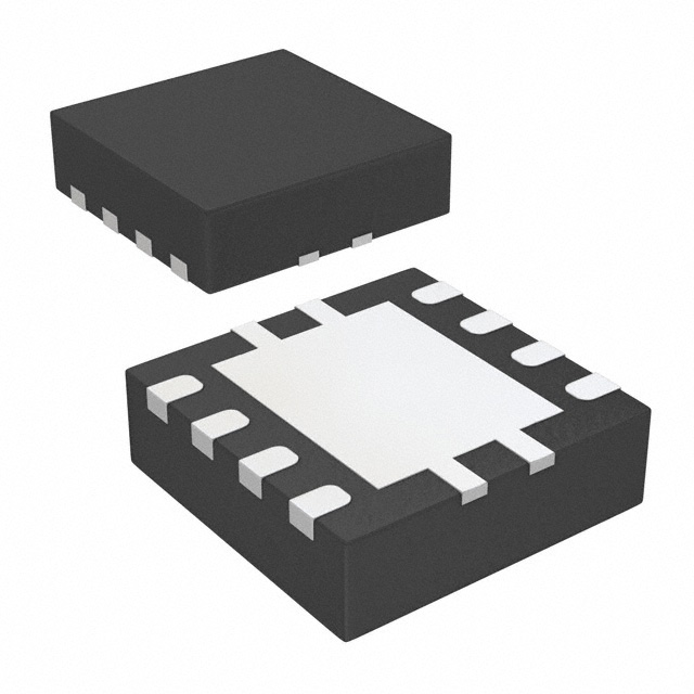
- Part No.:
- TPS7A8012DRBR
- Manufacturer:
- Texas Instruments
- Package:
- 8-VDFN Exposed Pad
- Datasheet:
-
 TPS7A8012DRBR.pdf
- Description:
- IC REG LINEAR 1.2V 1A 8SON
- Quantity:
- Payment:

- Shipping:

Inventory:2,508
Please send an inquiry. Send us your inquiry, and we will respond immediately.
Product details
Overview
TPS7A8012DRBR from Texas Instruments is a fixed-output, 1.2-V, 1-A low-dropout linear regulator with PMOS pass device, 500-mV dropout at 1 A, 63-dB PSRR at 1 kHz, and 14.3 × VOUT μVRMS output noise (100 Hz–100 kHz) using 0.01-μF NR capacitor. It delivers stable power to high-speed analog circuitry in telecom infrastructure and PLL/VCO supplies.
For engineers reviewing the TPS7A8012DRBR datasheet, TPS7A8012DRBR pinout, TPS7A8012DRBR application, or TPS7A8012DRBR equivalent, key selection criteria include guaranteed 3% output accuracy over –40°C to +125°C, compatibility with 4.7-μF ceramic output capacitors, thermal shutdown at 160°C, and enable-controlled shutdown with 2-μA quiescent current.
Technical Context
The TPS7A8012DRBR employs a BiCMOS process with a PMOS pass transistor to achieve low noise and high PSRR across 100 Hz–1 MHz. Its feedback loop uses an internal 1.243-V reference and SNS pin for output voltage sensing, eliminating external resistors.
It integrates quick-start circuitry that charges the NR capacitor via a 33-kΩ path for ~2 ms, then switches to a 250-kΩ RC filter for noise reduction. The device features undervoltage lockout (UVLO) with 1.98-V threshold and 75-mV hysteresis, plus foldback current limiting and thermal shutdown.
Key Specifications
| Parameter | Value and Actual Design Meaning |
|---|---|
| Output Voltage | Fixed 1.2 V ±3% over full load/line/temp range - ensures stable bias for precision analog blocks without external resistor network. |
| Max Output Current | 1 A continuous - supports single-rail powering of FPGA I/O banks or RF front-end ICs. |
| Dropout Voltage | 500 mV at 1 A - enables operation from 1.7-V input, suitable for Li-ion single-cell or post-buck intermediate rails. |
| PSRR | 63 dB at 1 kHz, 57 dB at 100 kHz - suppresses switching noise from upstream DC/DC converters feeding sensitive PLLs. |
| Output Noise | 14.3 × VOUT = 17.2 μVRMS (100 Hz–100 kHz) with 0.01-μF NR cap - meets low-noise requirements for ADC reference supplies and audio DACs. |
| Accuracy | ±0.3% typical at 100–500 mA, –3% to +3% worst-case - supports tight-tolerance digital core rails in industrial controllers. |
| Operating Temp | –40°C to +125°C junction - qualified for under-hood automotive modules and base station power stages. |
Pinout & Package
TPS7A8012DRBR is housed in a thermally enhanced 3-mm × 3-mm VSON-8 (DRB) package with exposed thermal pad. Pin 4 and the underside pad are GND; pins 1–2 and 7–8 are paralleled OUT and IN respectively for low-impedance routing.
| Pin/Terminal | Circuit Role | Design Meaning |
|---|---|---|
| IN (pins 7,8) | Unregulated input supply | Parallel connection reduces trace resistance and improves current sharing; accepts 2.2–6.5 V input. |
| OUT (pins 1,2) | Regulated output | Parallel pins lower output impedance; requires ≥4.7-μF ceramic capacitor on PCB for stability. |
| GND (pin 4 + pad) | Power ground reference | Exposed thermal pad must be soldered to PCB ground plane for RθJB = 23.4°C/W thermal performance. |
| EN (pin 5) | Enable control input | Active-high TTL/CMOS-compatible; drives high (>1.35 V at VIN >3.6 V) to activate regulator. |
| SNS (pin 3) | Output voltage sense | Direct connection to load improves regulation accuracy under high-current PCB trace IR drop. |
| NR (pin 6) | Noise reduction node | Accepts 1–100 nF capacitor to reduce bandgap reference noise; sets soft-start ramp time via RC time constant. |
Key Features
| Feature | Design Value |
|---|---|
| Wide-bandwidth high PSRR | Maintains >57 dB rejection up to 100 kHz - critical for isolating PLLs from noisy digital supply domains. |
| Low-noise architecture | 17.2 μVRMS output noise with 0.01-μF NR cap - eliminates need for secondary LC filtering in audio signal chains. |
| Quick-start NR charging | 33-kΩ start-up path charges CNR in ~2 ms - prevents slow VOUT ramp that could cause system boot failure. |
| Thermal & current protection | 160°C shutdown with 20°C hysteresis and foldback current limit - enables robust operation in sealed enclosures. |
| Ultra-low shutdown current | 2 μA max at 85°C - preserves battery life in always-on IoT sensor nodes powered by TPS7A8012DRBR. |
Applications
| Telecom Infrastructure | Audio Signal Processing |
|---|---|
Use Scenario: Powering RF transceiver synthesizers and baseband ADC/DACs in 5G small cells. IC Role / Device Role / Timing Role: Low-noise 1.2-V supply for VCO tuning voltage and ADC reference buffers. Use Value: 63-dB PSRR at 1 kHz rejects switching ripple from adjacent 1-MHz buck converters, preventing phase noise degradation. | Use Scenario: Supplying high-resolution audio CODECs in professional mixing consoles. IC Role / Device Role / Timing Role: Clean 1.2-V rail for analog front-end op-amps and sigma-delta modulators. Use Value: 17.2 μVRMS noise floor ensures <110-dB SNR in 24-bit/192-kHz audio paths without additional filtering. |
| High-Speed Interface (PLL/VCO) | Industrial Control Systems |
Use Scenario: Biasing clock multiplier PLLs in FPGA-based motor control gate drivers. IC Role / Device Role / Timing Role: Stable 1.2-V supply for PLL charge pump and loop filter op-amps. Use Value: 3% output accuracy over –40°C to +125°C maintains jitter <1 ps RMS across ambient temperature swings. | Use Scenario: Powering isolated CAN transceivers and real-time microcontroller cores in factory automation PLCs. IC Role / Device Role / Timing Role: Primary 1.2-V logic rail for ARM Cortex-M7 MCU and CAN FD PHY. Use Value: Thermal shutdown at 160°C prevents latch-up during extended 85°C ambient operation in enclosed cabinets. |
Equivalent & Alternatives
The following parts are listed as comparable options for similar LDO regulator applications.
| Alternative Part | Technical Difference | Application Difference | Selection Advice |
|---|---|---|---|
| TPS7A8112DRBR | Same 1.2-V fixed output, but 1.5-A rating and higher 650-mV dropout at 1.5 A; identical pinout and package. | Supports higher-current loads like multi-channel ADCs; requires larger input headroom. | Select when >1 A peak load is needed and board layout allows marginally higher dropout. |
| LP5907MFX-1.2/NOPB | 1.2-V fixed, 250-mA output, 120-mV dropout at 250 mA; SOT-23-5 package, no SNS or NR pins. | Limited to ultra-low-power sensors; lacks remote sensing and noise-reduction capability. | Choose only for space-constrained, sub-250-mA applications where PSRR >50 dB above 10 kHz is not required. |
Compared with TPS7A8012DRBR, TPS7A8112DRBR offers higher current capacity at the cost of increased dropout, while LP5907MFX-1.2/NOPB trades performance and feature set for footprint reduction and lower cost in low-power roles.
Availability
TPS7A8012DRBR is available at Aetrix Electronics and suitable for telecom infrastructure, audio signal processing, high-speed interface (PLL/VCO), and industrial control systems requiring stable component supply across extended temperature ranges and long production lifecycles.
Supply support for TPS7A8012DRBR includes scheduled delivery planning, volume procurement assistance, BOM continuity management, traceable sourcing, and lifecycle availability coordination for OEM customers, industrial embedded developers, connected-device designers, and electronics production programs.
Manufacturer
Texas Instruments is a global semiconductor leader delivering analog and embedded processing solutions, with over 90 years of innovation in power management ICs.
The TPS7A80 family was designed specifically for noise-sensitive, wide-bandwidth applications such as PLL/VCO power, high-speed data converters, and RF signal chains where PSRR and output noise directly impact system-level jitter and SNR.
FAQ
What is the minimum input voltage required for stable operation of the TPS7A8012DRBR?
The TPS7A8012DRBR requires a minimum input voltage of 2.2 V per its Recommended Operating Conditions. This ensures proper UVLO release and stable regulation even at maximum dropout (500 mV), allowing operation down to 1.7 V output headroom. Below 2.2 V, the device may enter undervoltage lockout and cease regulation.
Can the TPS7A8012DRBR be used without the NR capacitor?
Yes, the TPS7A8012DRBR functions without the NR capacitor, but output noise increases to 14.6 × VOUT μVRMS (≈17.5 μVRMS). The NR pin is left floating or grounded if noise reduction is not required; however, omitting the capacitor forfeits the soft-start benefit and degrades PSRR above 10 kHz.
How does the SNS pin improve regulation accuracy in the TPS7A8012DRBR?
The SNS pin in the TPS7A8012DRBR provides remote output voltage sensing at the load, compensating for IR drop across PCB traces. By connecting SNS directly to the load's VCC pin, the feedback loop maintains ±0.3% accuracy at the point of use - critical for high-current, low-voltage rails where trace resistance causes measurable voltage loss.
Is the TPS7A8012DRBR compatible with ceramic output capacitors smaller than 4.7 μF?
No - the TPS7A8012DRBR is only guaranteed stable with ≥4.7-μF ceramic output capacitance, as specified in the datasheet. Using smaller values risks oscillation due to insufficient phase margin; tantalum or aluminum electrolytic alternatives are not recommended due to ESR and aging effects.
What thermal derating applies to the TPS7A8012DRBR at 125°C ambient?
At 125°C ambient, the TPS7A8012DRBR's maximum continuous output current is limited by thermal constraints. With RθJA = 47.8°C/W and 160°C thermal shutdown, the safe dissipation limit is ~0.73 W - corresponding to ~0.6 A at 1.2 V output with 2.2 V input (1-V dropout). Board-level copper area significantly impacts actual capability.
TPS7A8012DRBR Specifications
- Product attributes
- Attribute value
- Manufacturer:
- Texas Instruments
- Series:
- -
- Package/Case:
- 8-VDFN Exposed Pad
- Packaging:
- Tape & Reel (TR)
- Product Status:
- Active
- Output Configuration:
- Positive
- Output Type:
- Fixed
- Number of Regulators:
- 1
- Voltage - Input (Max):
- 6.5V
- Voltage - Output (Min/Fixed):
- 1.2V
- Voltage - Output (Max):
- -
- Voltage Dropout (Max):
- 0.5V @ 1A
- Current - Output:
- 1A
- Current - Quiescent (Iq):
- 120 µA
- Current - Supply (Max):
- 350 µA
- PSRR:
- 48dB ~ 38dB (100Hz ~ 1MHz)
- Control Features:
- Enable
- Protection Features:
- Over Current, Over Temperature, Reverse Polarity, Under Voltage Lockout (UVLO)
- Operating Temperature:
- -40°C ~ 125°C (TJ)
- Grade:
- -
- Qualification:
- -
- Mounting Type:
- Surface Mount
- Supplier Device Package:
- 8-SON (3x3)
TPS7A8012DRBR FAQ
1.How can I place an order for TPS7A8012DRBR through Aetrix?
Please submit a Request for Quotation (RFQ) for TPS7A8012DRBR on Aetrix. Our sales agent will provide a competitive quotation and guide you through the order confirmation once you accept the terms.
2.Are the price and stock information for TPS7A8012DRBR reliable?
The price and inventory of TPS7A8012DRBR are updated periodically and may fluctuate due to market conditions. Stock and pricing data are typically refreshed every 24 hours. Quotation validity for TPS7A8012DRBR is usually 5 days.
3.What payment methods are accepted for TPS7A8012DRBR?
We accept Wire Transfer, PayPal, Credit Card, Western Union, MoneyGram, and Escrow for TPS7A8012DRBR transactions.
Note: Certain payment methods may incur a processing fee.
4.How is shipping managed for TPS7A8012DRBR?
TPS7A8012DRBR orders can be shipped via leading logistics carriers, including DHL, UPS, FedEx, TNT, or Registered Mail.
Once your TPS7A8012DRBR order is processed, you will receive an email with the shipment details and tracking number.
Note: Tracking information may take up to 24 hours to appear. Express delivery typically takes 3–5 business days.
5.How can I obtain technical support or documentation for TPS7A8012DRBR?
For technical support, including TPS7A8012DRBR datasheets, pinout diagrams, or application guidance, please contact our engineering support team. They can provide detailed documentation and assistance for your TPS7A8012DRBR requirements.
6.How does Aetrix verify that TPS7A8012DRBR is sourced from the original manufacturer or authorized distributors?
All TPS7A8012DRBR products on Aetrix are procured from qualified distributors and authorized channels. Our dedicated quality assurance team conducts strict verification, including traceability checks and, if necessary, third-party testing. This ensures that TPS7A8012DRBR meets industry standards.
7.What is the process for return or replacement of TPS7A8012DRBR?
All TPS7A8012DRBR units undergo pre-shipment inspection (PSI). If there is an issue with TPS7A8012DRBR, returns or replacements are accepted under the following conditions:
1.Quantity discrepancies, incorrect items, or visible external defects (such as breakage or corrosion), acknowledged by Aetrix.
2.The issue is reported within 90 days of delivery.
3.The TPS7A8012DRBR part is unused and in its original packaging.
Return procedure for TPS7A8012DRBR:
1.Submit a request within 90 days.
2.Obtain a Return Material Authorization (RMA) from Aetrix.
TPS7A8012DRBR Tags

-
MIC5504-1.8YM5-TR
Microchip Technology
-
MIC5504-3.3YM5-TR
Microchip Technology

-
MIC5365-3.0YC5-TR
Microchip Technology
-
MIC5365-1.8YC5-TR
Microchip Technology
-
MIC5365-2.5YC5-TR
Microchip Technology
-
MIC5365-3.3YC5-TR
Microchip Technology

-
MIC5365-3.3YD5-TR
Microchip Technology

-
MIC5317-3.3YM5-TR
Microchip Technology

-
TLV1117LV33DCYR
Texas Instruments

-
MIC5317-3.3YMT-TZ
Microchip Technology

-
MIC5528-3.3YMT-TR
Microchip Technology

-
TLV75801PDRVR
Texas Instruments
Tech Hub
A D latch stores one bit while Enable controls when data can pass. This reference covers gate-level operation, truth tables, transparency, setup and hold timing, LE versus OE, common ICs and practical …

An SR latch stores one bit through cross-coupled feedback. This engineering reference covers NOR and NAND implementations, truth tables, forbidden-state recovery, gated operation, switch debouncing, fa…

Latch circuits retain one bit through feedback. This technical reference covers SR and D latches, truth tables, transparency, timing limits, latch-versus-flip-flop behavior, applications and common log…

An engineering guide to LED driver operation, constant-current and constant-voltage outputs, linear and switching topologies, dimming, IC selection, calculations, replacement compatibility, and fault c…

Operational amplifier guide covering op amp basics, feedback, ideal vs real op amps, common configurations, buffer circuits, offset, bias current, gain-bandwidth, slew rate, rail-to-rail limits and sel…

Jumper cables guide covering safe connection order, red and black clamp placement, final ground connection, cable gauge, length, clamp quality, copper vs CCA cables, jump starter comparison and battery…

LDO regulator guide covering low dropout voltage, power dissipation, thermal design, PSRR, output noise, capacitor stability, adjustable LDO circuits, LDO vs buck converter and datasheet selection chec…

Conditional Access Module guide covering CAM meaning, CI/CI+ interface, smart card authorization, DVB security workflow, TV and set-top box compatibility, internal electronics, ESD protection, connecto…

Guide to electronic component obsolescence covering EOL risk, PCN/PDN notices, last-time buy planning, replacement options, form-fit-function validation, counterfeit risk and BOM lifecycle management.

18650 battery guide covering lithium-ion cell basics, 3.6V/3.7V voltage, 4.2V charging, mAh and Wh capacity, protected cells, chargers, BMS, series-parallel packs, holders, welding and sourcing checks.…


