
 My Inquiry
 My Account


Texas Instruments TS3A227EYFFR
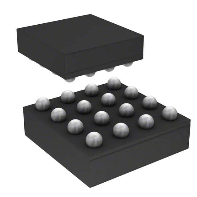
- Part No.:
- TS3A227EYFFR
- Manufacturer:
- Texas Instruments
- Category:
- Audio Special Purpose
- Package:
- 16-UFBGA, DSBGA
- Datasheet:
-
 TS3A227EYFFR.pdf
- Description:
- IC DETECTION SWITCH 16DSBGA
- Quantity:
- Payment:

- Shipping:

Inventory:4,465
Please send an inquiry. Send us your inquiry, and we will respond immediately.
Product details
Overview
TS3A227EYFFR from Texas Instruments is an autonomous audio accessory detection and configuration switch for 3.5 mm TRS/TRRS jacks, supporting stereo headphone, OMTP, and CTIA headset standards with 60 mΩ ground FET RON, 2.5 V–4.5 V supply range, and integrated key press detection for up to 4 buttons - deployed in mobile phones and tablets to eliminate insertion click/pop noise and enable FM antenna sharing via GNDA.
For engineers reviewing the TS3A227EYFFR datasheet, TS3A227EYFFR pinout, TS3A227EYFFR application, or TS3A227EYFFR equivalent, this page delivers verified electrical characteristics (e.g., 90 ms default insertion debounce, 175–210 ms detection sequence), package-specific thermal metrics (DSBGA YFF: θJA = 77.9°C/W), I²C timing compliance (up to 400 kHz fast mode), and confirmed FM transmission capability via GNDA routing.
Technical Context
The TS3A227EYFFR implements autonomous analog switching logic with dual-path ground FETs (RING2/SLEEVE) and depletion FETs for unpowered jack grounding, enabling seamless 3-pole/4-pole accessory identification without host CPU intervention. Its detection engine uses DET_TRIGGER edge-triggered initiation and internal voltage-sense comparators on GND_SENSE, RING2_SENSE, and SLEEVE_SENSE lines to distinguish OMTP vs. CTIA configurations.
Manual I²C control (SCL/SDA) allows runtime reconfiguration of debounce timers, switch states, and FM support bit, while isolation switches (S1/S2) disconnect MICBIAS from the jack during insertion/removal to suppress transient noise. Power-off operation is sustained by depletion FETs that maintain low-impedance ground paths even when VDD = 0 V.
Key Specifications
| Parameter | Value and Actual Design Meaning |
|---|---|
| Supply Voltage | 2.5 V to 4.5 V - enables direct integration with single-cell Li-ion battery rails without LDO. |
| Ground FET RON | 60 mΩ (QFN) / 40–85 mΩ (DSBGA) - minimizes crosstalk and preserves audio signal integrity in ground-return paths. |
| Detection Sequence Time | 175–210 ms - defines maximum latency between DET_TRIGGER assertion and INT assertion for system interrupt handling. |
| I²C Interface Speed | Up to 400 kHz Fast Mode - supports real-time switch reconfiguration without blocking audio data paths. |
| Quiescent Current (No Accessory) | 0.5–10 µA - ensures negligible battery drain during standby in always-on portable devices. |
| FM Transmission Support | Enabled via GNDA pin and I²C FM bit - allows shared use of sleeve/ring2 ground line as FM antenna return path. |
| ESD Rating (TIP/DET_TRIGGER) | ±8 kV Contact Discharge (IEC 61000-4-2) - protects against user-handling ESD events at jack interface points. |
Pinout & Package
TS3A227EYFFR is packaged in a 16-pin DSBGA (YFF) with 1.79 mm × 1.79 mm body size and 0.4 mm pitch. The package features bottom-side solder balls and requires PCB thermal pad connection to system ground for optimal thermal performance.
| Pin/Terminal | Circuit Role | Design Meaning |
|---|---|---|
| DET_TRIGGER (B1) | Edge-triggered detection initiator | Falling-edge input that starts autonomous accessory detection sequence; internal 0.5–1.85 MΩ pull-up enables simple jack-sense resistor implementation. |
| INT (C2) | Open-drain interrupt output | Asserts low upon completed detection, removal, or key press - requires external pull-up; cleared after host reads interrupt register. |
| MIC_PRESENT (A1) | Microphone presence indicator | Open-drain output pulled low when 4-pole headset is detected - signals host to enable MICP bias and key detection logic. |
| TIP (C1), RING2 (D1), SLEEVE (D3) | Audio jack contact interfaces | Direct connections to 3.5 mm jack TIP/RING2/SLEEVE pins; routed internally to S3PS/S3PR/S3GS/S3GR switches and sense circuitry. |
| GND_SENSE (A4), RING2_SENSE (C4), SLEEVE_SENSE (D4) | Accessory ground topology sensors | Analog sense inputs that identify OMTP vs. CTIA configuration by measuring impedance network topology across sleeve/ring2/mic paths. |
| GNDA (D2) | FM-capable ground FET return | Separate ground terminal for RING2/SLEEVE GNDFETs; connects to FM matching network when FM bit = 1, otherwise tied to system GND. |
| VDD (A3), GND (A2/B2) | Power and primary ground | VDD accepts 2.5–4.5 V with mandatory local decoupling; GND provides reference for all analog/digital circuits and thermal pad attachment. |
Key Features
| Feature | Design Value |
|---|---|
| Autonomous 3-/4-pole accessory detection | Eliminates need for host CPU polling or firmware-driven jack sensing - reduces software overhead and boot-time latency. |
| Adjustable insertion debounce timing | Configurable via I²C to reject mechanical bounce without external RC components - saves PCB area and BOM cost. |
| Ultra-low RON ground FETs (60 mΩ) | Preserves THD < 0.003% and SNR > –90 dB across 20 Hz–20 kHz - critical for high-fidelity mobile audio playback. |
| Power-off ground continuity | Depletion FETs maintain ≤150 Ω path from RING2/SLEEVE to GND when VDD = 0 V - prevents audible hum during cold-plug events. |
| Integrated key press detection (4 keys) | Measures resistance changes across TIP/RING2/SLEEVE to detect button presses/releases - enables headset remote functionality without ADC. |
Applications
| Mobile Handset Audio Jack Management | Tablet Headset Configuration |
|---|---|
|
Use Scenario: Detecting and routing microphone and ground paths for CTIA/OMTP headsets inserted into a 3.5 mm jack on a smartphone. IC Role / Device Role / Timing Role: Autonomous analog switch and configuration detector that identifies plug type, routes MICP/GNDA, and asserts INT within 210 ms. Use Value: Enables universal headset compatibility without hardware jumpers or manual user selection - improves out-of-box experience and reduces support calls. |
Use Scenario: Managing audio path isolation during headset insertion/removal in a tablet to prevent click/pop noise in speakers or earpieces. IC Role / Device Role / Timing Role: Isolation controller using S1/S2 switches to disconnect MICBIAS before mechanical contact closure, suppressing transients. Use Value: Achieves >90 dB PSRR at 217 Hz and >–75 dB channel separation - eliminates audible artifacts during hot-plug events. |
| Notebook Audio Jack with FM Antenna Sharing | Ultrabook Key Press Remote Support |
|
Use Scenario: Using the headset ground line as an FM antenna return path in a Windows notebook with integrated FM radio. IC Role / Device Role / Timing Role: FM transmission enabler via GNDA pin routing and I²C-controlled FM bit activation - maintains audio ground integrity while enabling RF path. Use Value: Eliminates need for separate FM antenna trace - reduces layer count and improves RF efficiency through shared ground conductor. |
Use Scenario: Detecting volume up/down and play/pause button presses on a 4-pole headset connected to an ultrabook. IC Role / Device Role / Timing Role: Resistive key scanner using TIP/RING2/SLEEVE voltage dividers and internal ADC-less comparison logic. Use Value: Supports 4-key matrix with press/release detection - enables media control without dedicated microcontroller or additional I/O pins. |
Equivalent & Alternatives
The following parts are listed as comparable options for similar audio accessory detection and configuration applications.
| Alternative Part | Technical Difference | Application Difference | Selection Advice |
|---|---|---|---|
| TS3A226AEYFFR | Supports only 3-pole accessories; lacks RING2_SENSE/SLEEVE_SENSE pins and OMTP detection logic. | Restricted to stereo headphone use; cannot route microphone or support headset remotes. | Select when only TRS detection is required and cost sensitivity outweighs 4-pole flexibility. |
| MAX14525ETA+T | Higher 120 mΩ ground FET RON; no integrated key press detection; requires external debounce RC network. | Lower audio fidelity (THD up to 0.01%) and increased PCB footprint due to external components. | Choose where I²C control is unnecessary and legacy design reuse favors Maxim's pinout compatibility. |
Compared with TS3A227EYFFR, TS3A226AEYFFR omits 4-pole support and key detection, limiting it to basic headphone switching, while MAX14525ETA+T trades higher distortion and external component dependency for broader vendor availability - TS3A227EYFFR remains optimal for universal headset compatibility with minimal BOM impact.
Availability
TS3A227EYFFR is available at Aetrix Electronics and suitable for mobile handsets, tablets, and ultrabooks requiring stable component supply, universal 3.5 mm headset support, and FM antenna sharing capability.
Supply support for TS3A227EYFFR includes scheduled delivery planning, volume procurement assistance, BOM continuity management, traceable sourcing, and lifecycle availability coordination for OEM customers, industrial embedded developers, connected-device designers, and electronics production programs.
Manufacturer
Texas Instruments is a global semiconductor company headquartered in Dallas, Texas, specializing in analog and embedded processing technologies with over 90 years of innovation in power management, signal chain, and interface solutions.
The TS3A227EYFFR belongs to TI's Audio Interface Switch family, designed specifically for intelligent 3.5 mm jack management in battery-powered portable devices - prioritizing ultra-low quiescent current, autonomous operation, and multi-standard headset compatibility.
FAQ
What is the function of the DET_TRIGGER pin on the TS3A227EYFFR?
The DET_TRIGGER pin on the TS3A227EYFFR is an edge-sensitive input that initiates the autonomous accessory detection sequence upon a falling edge. It features an internal 0.5–1.85 MΩ pull-up resistor, allowing direct connection to a 3.5 mm jack switch contact. When the jack detects plug insertion, DET_TRIGGER is pulled low, starting the 90 ms default debounce timer and subsequent configuration analysis - eliminating the need for external RC networks or host polling.
Does the TS3A227EYFFR support both OMTP and CTIA headset standards?
Yes, the TS3A227EYFFR explicitly supports both OMTP and CTIA (also known as AHJ or standard TRRS) headset configurations. It uses dedicated sense pins - GND_SENSE, RING2_SENSE, and SLEEVE_SENSE - to measure impedance networks across the plug contacts and autonomously determine whether the microphone is on Ring2 (CTIA) or Sleeve (OMTP). This enables automatic routing of MICP and GNDA without host intervention or hardware configuration.
How does the TS3A227EYFFR reduce click/pop noise during headset insertion?
The TS3A227EYFFR reduces click/pop noise by isolating the MICBIAS voltage source from the audio jack using internal S1 and S2 switches before mechanical contact closure. During insertion, these switches open to break the DC path between codec MICBIAS and the jack, preventing transient currents that cause audible artifacts. After detection completes and routing is confirmed, the switches close - ensuring clean, silent hot-plug operation verified to achieve >90 dB PSRR at 217 Hz.
Can the TS3A227EYFFR be used for FM transmission in portable devices?
Yes, the TS3A227EYFFR supports FM transmission by routing the FM receiver's matching network through the GNDA pin. When the FM support bit is set to '1' via I²C, the ground FETs (RING2 GNDFET and SLEEVE GNDFET) become active conduction paths for FM signals, allowing the headset's ground line to serve as an antenna return. This eliminates the need for a separate FM antenna trace while maintaining audio ground integrity - a feature confirmed in TI's SCDS358B datasheet Section 9.1.
What is the quiescent current of the TS3A227EYFFR when no headset is inserted?
The TS3A227EYFFR draws only 0.5–10 µA of quiescent current when no headset is inserted and the I²C bus is inactive - measured at VDD = 2.5 V to 4.5 V. This ultra-low sleep-mode current is achieved by shutting down internal detection circuitry and disabling analog comparators, making it ideal for battery-constrained applications like smartphones and tablets where standby power budget is critical.
TS3A227EYFFR Specifications
- Product attributes
- Attribute value
- Manufacturer:
- Texas Instruments
- Series:
- -
- Package/Case:
- 16-UFBGA, DSBGA
- Packaging:
- Tape & Reel (TR)
- Product Status:
- Active
- Function:
- Detection Switch
- Applications:
- Consumer Audio
- Number of Channels:
- 1
- Interface:
- I2C
- Voltage - Supply:
- 2.5V ~ 4.5V
- Operating Temperature:
- -40°C ~ 85°C (TA)
- Specifications:
- -
- Mounting Type:
- Surface Mount
- Grade:
- -
TS3A227EYFFR FAQ
1.How can I place an order for TS3A227EYFFR through Aetrix?
Please submit a Request for Quotation (RFQ) for TS3A227EYFFR on Aetrix. Our sales agent will provide a competitive quotation and guide you through the order confirmation once you accept the terms.
2.Are the price and stock information for TS3A227EYFFR reliable?
The price and inventory of TS3A227EYFFR are updated periodically and may fluctuate due to market conditions. Stock and pricing data are typically refreshed every 24 hours. Quotation validity for TS3A227EYFFR is usually 5 days.
3.What payment methods are accepted for TS3A227EYFFR?
We accept Wire Transfer, PayPal, Credit Card, Western Union, MoneyGram, and Escrow for TS3A227EYFFR transactions.
Note: Certain payment methods may incur a processing fee.
4.How is shipping managed for TS3A227EYFFR?
TS3A227EYFFR orders can be shipped via leading logistics carriers, including DHL, UPS, FedEx, TNT, or Registered Mail.
Once your TS3A227EYFFR order is processed, you will receive an email with the shipment details and tracking number.
Note: Tracking information may take up to 24 hours to appear. Express delivery typically takes 3–5 business days.
5.How can I obtain technical support or documentation for TS3A227EYFFR?
For technical support, including TS3A227EYFFR datasheets, pinout diagrams, or application guidance, please contact our engineering support team. They can provide detailed documentation and assistance for your TS3A227EYFFR requirements.
6.How does Aetrix verify that TS3A227EYFFR is sourced from the original manufacturer or authorized distributors?
All TS3A227EYFFR products on Aetrix are procured from qualified distributors and authorized channels. Our dedicated quality assurance team conducts strict verification, including traceability checks and, if necessary, third-party testing. This ensures that TS3A227EYFFR meets industry standards.
7.What is the process for return or replacement of TS3A227EYFFR?
All TS3A227EYFFR units undergo pre-shipment inspection (PSI). If there is an issue with TS3A227EYFFR, returns or replacements are accepted under the following conditions:
1.Quantity discrepancies, incorrect items, or visible external defects (such as breakage or corrosion), acknowledged by Aetrix.
2.The issue is reported within 90 days of delivery.
3.The TS3A227EYFFR part is unused and in its original packaging.
Return procedure for TS3A227EYFFR:
1.Submit a request within 90 days.
2.Obtain a Return Material Authorization (RMA) from Aetrix.
TS3A227EYFFR Tags

-
SA571DR2G
onsemi
-
ADAU7002ACBZ-R7
Analog Devices Inc.

-
DRV135UA/2K5
Texas Instruments

-
DRV134UA/1K
Texas Instruments

-
DRV134PA
Texas Instruments
-
DRV134UA
Texas Instruments
-
DRV135UA
Texas Instruments
-
SA572DR2G
onsemi
-
PGA2311U/1K
Texas Instruments
-
SI8244BB-D-IS1R
Skyworks Solutions Inc.

-
CS8416K-CZZR
Cirrus Logic Inc.
-
SRC4392IPFBR
Texas Instruments
Tech Hub

A practical engineering guide to 3.3V and 5V logic compatibility, input thresholds, resistor dividers, translator ICs, MOSFET level shifting, I2C pull-ups, timing limits and power-sequencing risks.

The 74HC595 uses push-pull logic outputs, while the TPIC6B595 uses 50 V open-drain DMOS sinks for higher-power loads. This guide compares timing, current limits, 3.3 V interfacing, load wiring, thermal…

The 74HC595 converts serial data into eight stable parallel outputs. This guide covers pin functions, shift and storage timing, OE and MR behavior, drive-current limits, cascading, voltage compatibilit…

A technical comparison of level-sensitive latches and edge-triggered flip-flops, covering timing windows, setup and hold limits, master–slave operation, time borrowing, race-through, HDL inference and…

A D latch stores one bit while Enable controls when data can pass. This reference covers gate-level operation, truth tables, transparency, setup and hold timing, LE versus OE, common ICs and practical …

An SR latch stores one bit through cross-coupled feedback. This engineering reference covers NOR and NAND implementations, truth tables, forbidden-state recovery, gated operation, switch debouncing, fa…

Latch circuits retain one bit through feedback. This technical reference covers SR and D latches, truth tables, transparency, timing limits, latch-versus-flip-flop behavior, applications and common log…

An engineering guide to LED driver operation, constant-current and constant-voltage outputs, linear and switching topologies, dimming, IC selection, calculations, replacement compatibility, and fault c…

Operational amplifier guide covering op amp basics, feedback, ideal vs real op amps, common configurations, buffer circuits, offset, bias current, gain-bandwidth, slew rate, rail-to-rail limits and sel…

Jumper cables guide covering safe connection order, red and black clamp placement, final ground connection, cable gauge, length, clamp quality, copper vs CCA cables, jump starter comparison and battery…


