
 My Inquiry
 My Account


Texas Instruments TSB12LV01APZ
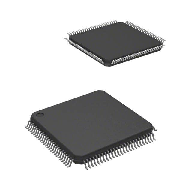
- Part No.:
- TSB12LV01APZ
- Manufacturer:
- Texas Instruments
- Category:
- Controllers
- Package:
- 100-LQFP
- Datasheet:
-
 TSB12LV01APZ.pdf
- Description:
- IC HP 3.3V LINK LAYER 100LQFP
- Quantity:
- Payment:

- Shipping:

Inventory:39,248
Please send an inquiry. Send us your inquiry, and we will respond immediately.
Product details
Overview
TSB12LV01APZ from Texas Instruments is a IEEE 1394-1995 (FireWire) link-layer controller IC that bridges 32-bit host buses to 1394 physical-layer devices. It supports 100/200/400 Mbit/s data rates, implements full CRC-32 generation and verification, operates as cycle master, and integrates 2-KB configurable FIFOs for asynchronous, isochronous, and general receive operations - enabling high-speed digital video/audio I/O subsystems in PC add-in cards and consumer electronics.
For engineers reviewing the TSB12LV01APZ datasheet, TSB12LV01APZ pinout, TSB12LV01APZ application, or TSB12LV01APZ equivalent, key selection criteria include IEEE 1394-1995 compliance, 32-bit host bus timing at up to 50 MHz BCLK, PHY interface compatibility with TI TSB11LV01/TSB21LV03A, and support for dual-channel isochronous reception with programmable packet/block interrupt triggers.
Technical Context
The TSB12LV01APZ implements a dedicated link-layer controller architecture per IEEE 1394-1995 Annex J, with separate transmit/receive FIFOs (ATF, ITF, GRF), cycle timer, cycle monitor, and CRC-32 engine. Its PHY interface uses CTL0/CTL1 control lines and D0–D7 bidirectional data lines to manage bus arbitration, status exchange, and packet transfers with compliant PHY chips.
Host communication occurs via a generic 32-bit synchronous bus using CS/WR/CA signals and BCLK timing; register access and FIFO data movement are interrupt-driven. The device supports burst-mode transfers at up to one quadlet per BCLK cycle and includes internal logic to detect lost cycle-start messages and handle self-ID packet reception.
Key Specifications
| Parameter | Value and Actual Design Meaning |
|---|---|
| Standard Compliance | IEEE 1394-1995 (FireWire 400) link-layer protocol, including isochronous, asynchronous, and self-ID packet handling. |
| Data Rates | 100 Mbit/s, 200 Mbit/s, and 400 Mbit/s - selectable per PHY negotiation; D0–D7 used fully only at 400 Mbit/s. |
| FIFO Memory | 2 KB on-chip RAM configurable as GRF (general receive), ATF (asynchronous transmit), and ITF (isochronous transmit) with independent sizing. |
| Host Interface | 32-bit multiplexed address/data bus with CS/WR/CA handshaking; supports burst writes/reads at ≤50 MHz BCLK (200 MB/s peak). |
| CRC Engine | Hardware CRC-32 generator and checker applied to all transmitted and received packets per IEEE 1394 specification. |
| Operating Voltage | 3.3 V core supply with 5-V tolerant inputs - enables direct interfacing to legacy 5-V host bus systems without level shifters. |
| Temperature Range | –40°C to +85°C industrial grade operation, validated for sustained use in embedded media interfaces. |
Pinout & Package
TSB12LV01APZ is housed in a 100-pin Thin Quad Flat Package (TQFP), designated PZ package, with 0.5-mm lead pitch and exposed thermal pad. Pin assignments follow JEDEC MO-137AC standard layout.
| Pin/Terminal | Circuit Role | Design Meaning |
|---|---|---|
| ADDR0–ADDR7 | Host address bus (LSBs) | Quadlet-aligned register/FIFO addressing; ADDR6/ADDR7 must be grounded per spec. |
| DATA0–DATA31 | Host bidirectional data bus | 32-bit wide path for configuration registers and FIFO data; MSB = DATA0. |
| CS / WR / CA | Host bus control signals | CS initiates transfer; WR selects read/write; CA confirms completion - enables synchronous register access. |
| INT | Interrupt output | Active-low signal indicating pending interrupts (e.g., FIFO full/empty, packet arrival, error); cleared by register write. |
| D0–D7 / CTL0 / CTL1 | PHY-link data and control | Bidirectional 8-bit data bus + 2-bit control bus per IEEE 1394 Annex J; integrated bus-hold buffers enable single-capacitor isolation. |
| CYCLEIN / CYCLEOUT | Cycle timing interface | Input for external cycle clock sync; output for cycle master timing distribution across multi-node 1394 networks. |
| RESET / POWERON / RAMEZ | Initialization controls | Asynchronous reset; power-on initialization flag; RAM erase control for FIFO memory clearing during startup. |
Key Features
| Feature | Design Value |
|---|---|
| Configurable FIFO allocation | User-definable GRF/ATF/ITF sizes allow optimization for asymmetric traffic profiles (e.g., large GRF for video capture, small ITF for control packets). |
| Programmable interrupt triggers | RxDta interrupt can fire per received packet or per programmable block boundary - critical for real-time buffer management when GRF < packet size. |
| Independent channel enable | Isochronous transmit/receive and asynchronous transmit can be enabled/disabled separately - simplifies power management and mode switching. |
| Burst-mode host throughput | One quadlet per BCLK cycle achievable in burst mode, enabling 200 MB/s peak host bandwidth at 50 MHz BCLK - matches FireWire 400 line rate. |
| PHY bus-hold isolation | Integrated bus-hold circuitry on CTL0/CTL1/Dx pins eliminates need for external pull-ups, reducing BOM cost and PCB area for capacitor-coupled PHY interfaces. |
Applications
| Digital Video Capture Card | Professional Audio Interface |
|---|---|
Use Scenario: Capturing uncompressed DV stream from camcorder into PC via PCIe or PCI add-in card. IC Role / Device Role / Timing Role: Link-layer controller managing 400 Mbit/s isochronous packet flow, cycle synchronization, and CRC validation between host memory and TSB11LV01 PHY. Use Value: Enables lossless real-time video ingestion with guaranteed bandwidth and deterministic latency via hardware-managed isochronous channels. | Use Scenario: Low-latency multichannel audio streaming between DAW and external FireWire audio interface. IC Role / Device Role / Timing Role: Cycle master coordinating time-sensitive isochronous transfers across two independent audio channels while handling asynchronous control commands. Use Value: Delivers sub-millisecond jitter performance and sample-accurate synchronization required for professional recording and monitoring. |
| Industrial Machine Vision System | Medical Imaging Workstation |
Use Scenario: High-resolution image acquisition from FireWire cameras in automated inspection equipment. IC Role / Device Role / Timing Role: Host-side link controller receiving large asynchronous image frames and isochronous trigger/status packets over shared 1394 bus. Use Value: Supports reliable frame delivery with CRC-32 error detection and configurable GRF depth to absorb variable camera exposure times. | Use Scenario: DICOM image transfer from ultrasound or MRI modalities to PACS server via FireWire-equipped diagnostic workstation. IC Role / Device Role / Timing Role: Secure, high-throughput link-layer interface handling large asynchronous DICOM files and time-stamped isochronous metadata streams. Use Value: Ensures data integrity through hardware CRC and provides deterministic interrupt response for time-critical imaging workflows. |
Equivalent & Alternatives
The following parts are listed as comparable options for similar IEEE 1394 link-layer controller applications.
| Alternative Part | Technical Difference | Application Difference | Selection Advice |
|---|---|---|---|
| TSB12LV01AI | Same silicon, extended temperature range (–40°C to +85°C vs. 0°C to +70°C for TSB12LV01APZ); identical pinout and functionality. | Required for industrial or automotive environments where ambient operating temperature exceeds 70°C. | Select TSB12LV01AI when extended thermal range is mandatory; otherwise TSB12LV01APZ suffices for commercial desktop applications. |
| TSB12C01A | Predecessor with known errata; lacks GRF cycle-start storage, independent channel enable, and optimized FIFO status registers present in TSB12LV01APZ. | Not recommended for new designs due to uncorrected functional limitations and absence of key enhancements. | TSB12LV01APZ replaces TSB12C01A in all new implementations; migration requires no PCB changes but leverages improved interrupt efficiency and reliability. |
Compared with TSB12C01A, TSB12LV01APZ delivers corrected errata, enhanced isochronous flexibility, and faster host-FIFO throughput - while TSB12LV01AI offers identical functionality with broader thermal qualification for harsher environments.
Availability
TSB12LV01APZ is available at Aetrix Electronics and suitable for digital video capture cards, professional audio interfaces, and industrial machine vision systems requiring stable component supply and long-term obsolescence management.
Supply support for TSB12LV01APZ includes scheduled delivery planning, volume procurement assistance, BOM continuity management, traceable sourcing, and lifecycle availability coordination for OEM customers, industrial embedded developers, connected-device designers, and electronics production programs.
Manufacturer
Texas Instruments is a global semiconductor leader specializing in analog, embedded processing, and connectivity solutions with decades of FireWire technology development.
The TSB12LV01APZ belongs to TI's IEEE 1394 link-layer controller product line, designed specifically to enable robust, high-bandwidth serial I/O in PC peripherals, broadcast equipment, and industrial imaging systems.
FAQ
What is the primary function of the TSB12LV01APZ in a FireWire system?
The TSB12LV01APZ serves as the IEEE 1394-1995 link-layer controller, handling packet assembly/disassembly, CRC-32 generation and checking, isochronous cycle management, and FIFO buffering between a 32-bit host bus and a 1394 PHY chip. It enables full FireWire 400 functionality without requiring external logic, making it central to host-side FireWire interface design.
Does the TSB12LV01APZ support both isochronous and asynchronous data transfers?
Yes, the TSB12LV01APZ natively supports both isochronous and asynchronous transfers per IEEE 1394-1995. It includes dedicated isochronous transmit and receive FIFOs, supports up to two isochronous channels simultaneously, and allows independent enable/disable control of each transfer type - a key capability confirmed in its feature set and register definitions.
What PHY devices is the TSB12LV01APZ compatible with?
The TSB12LV01APZ is explicitly designed to interface with TI's TSB11LV01, TSB14C01, TSB21LV03A, and TSB41LV0x family of PHY chips. Its CTL0/CTL1 signaling, D0–D7 data bus, and timing comply with IEEE 1394 Annex J, ensuring interoperability with any PHY adhering to that specification.
How does the TSB12LV01APZ handle interrupt generation for host CPU notification?
The TSB12LV01APZ uses an active-low INT pin driven by configurable interrupt sources including FIFO status (GRFEMP, ATF full/empty), packet arrival, cycle start detection, and error conditions. Interrupts are cleared by writing to the INT register, and RxDta can be programmed to assert on per-packet or per-block boundaries - providing precise host synchronization for real-time data handling.
What is the significance of the "PZ" suffix in TSB12LV01APZ?
The "PZ" suffix denotes the 100-pin Thin Quad Flat Package (TQFP) variant of the TSB12LV01A, specified for commercial temperature range (0°C to +70°C). It defines the mechanical footprint, lead count, and thermal characteristics - distinguishing it from other packages like "PI" (plastic DIP) or "PG" (PGA), and confirming compatibility with standard TQFP PCB layouts.
TSB12LV01APZ Specifications
- Product attributes
- Attribute value
- Manufacturer:
- Texas Instruments
- Package/Case:
- 100-LQFP
- Programmable:
- Not Verified
- Protocol:
- -
- Function:
- -
- Interface:
- -
- Standards:
- -
- Voltage - Supply:
- -
- Current - Supply:
- -
- Operating Temperature:
- -
- Supplier Device Package:
- 100-LQFP (14x14)
- Grade:
- -
- Qualification:
- -
TSB12LV01APZ FAQ
1.How can I place an order for TSB12LV01APZ through Aetrix?
Please submit a Request for Quotation (RFQ) for TSB12LV01APZ on Aetrix. Our sales agent will provide a competitive quotation and guide you through the order confirmation once you accept the terms.
2.Are the price and stock information for TSB12LV01APZ reliable?
The price and inventory of TSB12LV01APZ are updated periodically and may fluctuate due to market conditions. Stock and pricing data are typically refreshed every 24 hours. Quotation validity for TSB12LV01APZ is usually 5 days.
3.What payment methods are accepted for TSB12LV01APZ?
We accept Wire Transfer, PayPal, Credit Card, Western Union, MoneyGram, and Escrow for TSB12LV01APZ transactions.
Note: Certain payment methods may incur a processing fee.
4.How is shipping managed for TSB12LV01APZ?
TSB12LV01APZ orders can be shipped via leading logistics carriers, including DHL, UPS, FedEx, TNT, or Registered Mail.
Once your TSB12LV01APZ order is processed, you will receive an email with the shipment details and tracking number.
Note: Tracking information may take up to 24 hours to appear. Express delivery typically takes 3–5 business days.
5.How can I obtain technical support or documentation for TSB12LV01APZ?
For technical support, including TSB12LV01APZ datasheets, pinout diagrams, or application guidance, please contact our engineering support team. They can provide detailed documentation and assistance for your TSB12LV01APZ requirements.
6.How does Aetrix verify that TSB12LV01APZ is sourced from the original manufacturer or authorized distributors?
All TSB12LV01APZ products on Aetrix are procured from qualified distributors and authorized channels. Our dedicated quality assurance team conducts strict verification, including traceability checks and, if necessary, third-party testing. This ensures that TSB12LV01APZ meets industry standards.
7.What is the process for return or replacement of TSB12LV01APZ?
All TSB12LV01APZ units undergo pre-shipment inspection (PSI). If there is an issue with TSB12LV01APZ, returns or replacements are accepted under the following conditions:
1.Quantity discrepancies, incorrect items, or visible external defects (such as breakage or corrosion), acknowledged by Aetrix.
2.The issue is reported within 90 days of delivery.
3.The TSB12LV01APZ part is unused and in its original packaging.
Return procedure for TSB12LV01APZ:
1.Submit a request within 90 days.
2.Obtain a Return Material Authorization (RMA) from Aetrix.
TSB12LV01APZ Tags

-
PTN5150AHXMP
NXP Semiconductors

-
USB3740B-AI9-TR
Microchip Technology

-
USB3740B-AI2-TR
Microchip Technology

-
USB3300-EZK-TR
Microchip Technology
-
USB3300-EZK
Microchip Technology

-
FUSB340TMX
onsemi

-
FUSB302BMPX
onsemi

-
DP83826IRHBR
Texas Instruments

-
MCP2518FDT-E/QBB
Microchip Technology
-
FUSB302MPX
onsemi

-
MCP2518FDT-E/SL
Microchip Technology

-
FT260Q-R
FTDI, Future Technology Devices International Ltd
Tech Hub

A practical engineering guide to 3.3V and 5V logic compatibility, input thresholds, resistor dividers, translator ICs, MOSFET level shifting, I2C pull-ups, timing limits and power-sequencing risks.

The 74HC595 uses push-pull logic outputs, while the TPIC6B595 uses 50 V open-drain DMOS sinks for higher-power loads. This guide compares timing, current limits, 3.3 V interfacing, load wiring, thermal…

The 74HC595 converts serial data into eight stable parallel outputs. This guide covers pin functions, shift and storage timing, OE and MR behavior, drive-current limits, cascading, voltage compatibilit…

A technical comparison of level-sensitive latches and edge-triggered flip-flops, covering timing windows, setup and hold limits, master–slave operation, time borrowing, race-through, HDL inference and…

A D latch stores one bit while Enable controls when data can pass. This reference covers gate-level operation, truth tables, transparency, setup and hold timing, LE versus OE, common ICs and practical …

An SR latch stores one bit through cross-coupled feedback. This engineering reference covers NOR and NAND implementations, truth tables, forbidden-state recovery, gated operation, switch debouncing, fa…

Latch circuits retain one bit through feedback. This technical reference covers SR and D latches, truth tables, transparency, timing limits, latch-versus-flip-flop behavior, applications and common log…

An engineering guide to LED driver operation, constant-current and constant-voltage outputs, linear and switching topologies, dimming, IC selection, calculations, replacement compatibility, and fault c…

Operational amplifier guide covering op amp basics, feedback, ideal vs real op amps, common configurations, buffer circuits, offset, bias current, gain-bandwidth, slew rate, rail-to-rail limits and sel…

Jumper cables guide covering safe connection order, red and black clamp placement, final ground connection, cable gauge, length, clamp quality, copper vs CCA cables, jump starter comparison and battery…


