
 My Inquiry
 My Account


Texas Instruments TSB12LV01BIPZTEP
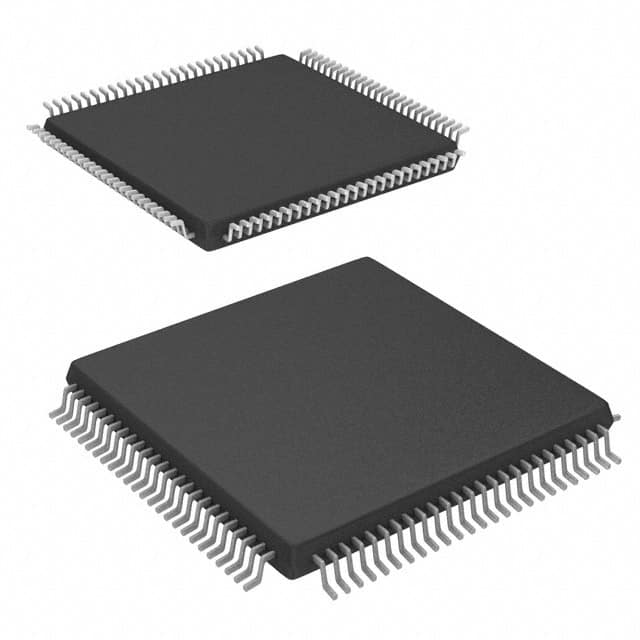
- Part No.:
- TSB12LV01BIPZTEP
- Manufacturer:
- Texas Instruments
- Category:
- Controllers
- Package:
- 100-TQFP
- Datasheet:
-
 TSB12LV01BIPZTEP.pdf
- Description:
- IC LINK LAYER 3.3V HP 100-TQFP
- Quantity:
- Payment:

- Shipping:

Inventory:3,652
Please send an inquiry. Send us your inquiry, and we will respond immediately.
Product details
Overview
TSB12LV01BIPZTEP from Texas Instruments is an IEEE 1394-1995 link-layer controller IC enabling high-speed serial bus connectivity between a 32-bit host bus and 1394 physical layer (PHY) devices. It supports 100/200/400 Mbits/s data rates, performs 32-bit CRC generation and verification, operates as cycle master, and manages three configurable FIFOs (ATF, ITF, GRF) totaling 2 KB on-die memory for asynchronous and isochronous transfers in digital video/audio I/O subsystems.
For engineers reviewing the TSB12LV01BIPZTEP datasheet, TSB12LV01BIPZTEP pinout, TSB12LV01BIPZTEP application, or TSB12LV01BIPZTEP equivalent, key selection criteria include its 100-pin PQFP package, 3.3-V core with 5-V tolerant inputs, IEEE 1394a–2000 timing compliance, dual-channel isochronous receive capability, and host interface clock duty-cycle constraints at 50 MHz.
Technical Context
The TSB12LV01BIPZTEP implements a full IEEE 1394 link-layer controller (LLC) with integrated PHY-link interface logic, supporting all four CTL-encoded operations (read/write register, bus request, acceleration control) per IEEE 1394-1995 Annex J. Its architecture includes dedicated transmit/receive FIFOs, cycle timer and monitor, and CRC engine operating across all supported speeds.
It interfaces via a generic 32-bit host bus with quadlet-aligned register access, interrupt-driven operation, and programmable general-purpose outputs (GPO0–GPO2). The device requires precise BCLK duty cycle (45–55% at 50 MHz) and lacks bus holder cells on the PHY interface-replacing ISO with VCC on pin 69 versus TSB12LV01A.
Key Specifications
| Parameter | Value and Actual Design Meaning |
|---|---|
| IEEE Standard | Compliant with IEEE 1394-1995 and IEEE 1394a–2000 timing requirements for PHY-link interface. |
| Data Rates | 100 / 200 / 400 Mbits/s - selectable per packet; D-bus width scales (D0–D1, D0–D3, D0–D7) accordingly. |
| FIFO Memory | 2 KB on-chip RAM configurable as ATF (asynchronous transmit), ITF (isochronous transmit), and GRF (general receive) FIFOs. |
| Host Interface | 32-bit parallel bus with CS/WR/CA control, quadlet-aligned register map, and active-low INT output. |
| Supply & Tolerance | 3.3-V core supply; all host bus inputs (ADDR/DATA/CS/WR/etc.) are 5-V tolerant - simplifies level-shifting in mixed-voltage systems. |
| Cycle Master | Full cycle master functionality including CycleStart generation, CycleIn/CycleOut synchronization, and lost-cycle detection. |
| Operating Temp | –40°C to +85°C industrial temperature range, qualified per JEDEC extended reliability standards (HAST, temp cycle, etc.). |
Pinout & Package
TSB12LV01BIPZTEP is housed in a 100-pin plastic quad flat pack (PQFP) with 0.65-mm lead pitch, designated PZT package per TI documentation. Pin 1 is located at bottom-left corner (top view); ADDR6/ADDR7 must be grounded; reserved pins tied to GND.
| Pin/Terminal | Circuit Role | Design Meaning |
|---|---|---|
| ADDR0–ADDR7 | Host address bus (MSB first) | Quadlet-aligned register/FIFO addressing; ADDR6/ADDR7 hardwired to GND per spec. |
| DATA0–DATA31 | Host bidirectional data bus | 32-bit wide; byte0 (DATA0–DATA7) = most significant byte; enables burst and quick-access modes. |
| CS, WR, CA | Host bus control signals | /CS initiates access; /WR selects read (high) or write (low); /CA confirms completion - enables glueless interfacing. |
| INT | Interrupt output | Active-low, open-drain capable; asserts on FIFO full/empty, CRC error, cycle start loss, or PHY status change. |
| D0–D7, CTL0/CTL1, LREQ, SCLK | PHY-link interface | 8-bit scalable data bus; 2-bit CTL encodes PHY operations; LREQ drives bus requests; SCLK clocks PHY status transfers. |
| CYCLEIN / CYCLEOUT | Cycle timing interface | Synchronizes isochronous streams: CYCLEIN receives cycle start from PHY; CYCLEOUT outputs local cycle reference. |
| GPO0–GPO2 (GRFEMP/CYDNE/CYST) | Programmable outputs | Configurable as status flags: GRFEMP = general FIFO empty; CYDNE = cycle done; CYST = cycle start asserted. |
Key Features
| Feature | Design Value |
|---|---|
| Integrated 2-KB FIFO memory | Eliminates external FIFOs; user-configurable partitioning among ATF, ITF, and GRF supports concurrent async/isochronous traffic. |
| Dual-channel isochronous receive | Enables simultaneous real-time streaming of two independent audio/video channels without host CPU intervention. |
| 32-bit CRC generation & checking | Hardware-accelerated 32-bit CRC per IEEE 1394 packet ensures data integrity at line rate up to 400 Mbits/s. |
| Programmable GPOs (GPO0–GPO2) | Three dedicated outputs replace legacy ISO pin; provide direct hardware visibility into FIFO state and cycle timing events. |
| 5-V tolerant host inputs | Allows direct connection to legacy 5-V logic families without level shifters - reduces BOM count and layout complexity. |
Applications
| Digital Camcorder Interface | Professional Audio Interface |
|---|---|
Use Scenario: High-bandwidth transfer of uncompressed DV video frames from camcorder sensor to host PC or editing system. IC Role / Device Role / Timing Role: Link-layer controller managing isochronous packetization, CRC, cycle synchronization, and host-to-PHY bridging. Use Value: Enables sustained 25-MB/s (200-Mbits/s) real-time streaming with guaranteed latency and zero packet loss under IEEE 1394 timing rules. |
Use Scenario: Multi-channel digital audio recording system connecting 16-channel AES/EBU or ADAT optical interfaces to workstation. IC Role / Device Role / Timing Role: Cycle master coordinating isochronous time slots across two independent audio streams with precise CYCLEIN/CYCLEOUT alignment. Use Value: Delivers sample-accurate synchronization across 32+ channels using hardware-managed isochronous bandwidth allocation. |
| Industrial Machine Vision System | Medical Imaging Workstation |
Use Scenario: High-resolution line-scan camera capturing 12-bit monochrome images at >100 MB/s for semiconductor inspection. IC Role / Device Role / Timing Role: Asynchronous transmitter handling large block reads from frame buffer while maintaining isochronous trigger timing. Use Value: Combines 400-Mbits/s raw pixel throughput with deterministic trigger response via CYST/CYDNE GPO signaling. |
Use Scenario: PACS (Picture Archiving and Communication System) workstation ingesting DICOM image sequences from ultrasound or MRI modalities. IC Role / Device Role / Timing Role: Dual-channel isochronous receiver buffering real-time video streams while offloading host CPU via interrupt-driven FIFO management. Use Value: Supports concurrent ingestion of two diagnostic video feeds (e.g., B-mode + Doppler) with sub-millisecond inter-stream skew. |
Equivalent & Alternatives
The following parts are listed as comparable options for similar IEEE 1394 link-layer controller applications.
| Alternative Part | Technical Difference | Application Difference | Selection Advice |
|---|---|---|---|
| TSB12LV01AIPZT | Pin-compatible predecessor; lacks GPO0–GPO2, no Mux/Host Control Registers (0x40/0x44), no BCLK duty-cycle restriction at 50 MHz. | Legacy designs requiring identical footprint but no enhanced GPO or register features; not suitable for new designs needing CYST/CYDNE signaling. | Select only if backward compatibility with existing TSB12LV01A PCBs is required and enhanced features are unused. |
| FW643-001 (Agere Systems) | Single-chip 1394a PHY+link controller; integrates PHY analog front-end; no separate PHY interface; 128-pin TQFP. | Reduces component count by eliminating discrete PHY; unsuitable where TI PHYs (e.g., TSB41AB1) or PHY-level diagnostics are required. | Choose when minimizing bill-of-materials and board space outweighs need for PHY-level register access and TI ecosystem integration. |
Compared with TSB12LV01AIPZT, TSB12LV01BIPZTEP adds critical GPOs for cycle timing visibility and stricter BCLK tolerance; compared with FW643-001, it retains modular PHY-link separation for testability and TI PHY interoperability - making it optimal for industrial systems requiring debuggable, field-upgradable 1394 links.
Availability
TSB12LV01BIPZTEP is available at Aetrix Electronics and suitable for digital video capture, professional audio streaming, industrial machine vision, and medical imaging applications requiring stable component supply, long-term lifecycle support, and guaranteed traceability.
Supply support for TSB12LV01BIPZTEP includes scheduled delivery planning, volume procurement assistance, BOM continuity management, traceable sourcing, and lifecycle availability coordination for OEM customers, industrial embedded developers, connected-device designers, and electronics production programs.
Manufacturer
Texas Instruments is a global semiconductor company specializing in analog, embedded processing, and connectivity solutions, with leadership in industrial, automotive, and communications infrastructure markets.
The TSB12LV01BIPZTEP belongs to TI's IEEE 1394 link-layer controller product line, designed specifically for high-reliability, real-time serial bus interfacing in professional media and industrial automation systems requiring deterministic isochronous performance.
FAQ
What is the primary function of the TSB12LV01BIPZTEP in a 1394 system?
The TSB12LV01BIPZTEP serves as the IEEE 1394 link-layer controller (LLC), managing packet formatting, CRC generation/checking, isochronous cycle timing, and host-to-PHY data flow. It bridges a 32-bit host bus to the 1394 physical layer, enabling 100/200/400 Mbits/s transfers. Unlike PHY-only devices, the TSB12LV01BIPZTEP handles protocol logic - making it essential for any system implementing full 1394 stack functionality without software-only LLC emulation.
Does the TSB12LV01BIPZTEP require an external PHY device?
Yes, the TSB12LV01BIPZTEP requires an external 1394 physical layer (PHY) device such as the TI TSB41AB1 or TSB41AB2. It provides the PHY-link interface (D0–D7, CTL0/CTL1, LREQ, SCLK) but contains no analog transceivers or cable drivers. This separation allows flexible PHY selection, diagnostic access to PHY registers via the TSB12LV01BIPZTEP's PHY-Chip Access Register (0x24), and compliance with IEEE 1394a–2000 timing specifications.
How does the TSB12LV01BIPZTEP handle isochronous data streams?
The TSB12LV01BIPZTEP supports reception on two independent isochronous channels with hardware-managed bandwidth allocation and cycle synchronization. It uses CYCLEIN to lock to incoming cycle-start messages from the PHY and generates CYCLEOUT for local timing. The isochronous receive FIFO (IRF) - configured within the 2 KB on-die memory - buffers packets with minimal CPU overhead, while GPO1 (CYDNE) and GPO2 (CYST) provide real-time hardware indicators of cycle boundaries for precise stream alignment.
What are the host interface timing requirements for the TSB12LV01BIPZTEP?
The TSB12LV01BIPZTEP requires a 3.3-V host bus clock (BCLK) with strict duty-cycle limits: at 50 MHz, duty cycle must be 45–55%; at ≤47 MHz, 40–60% is acceptable. Timing parameters include tACS (address setup to CS low) ≥15 ns, tCWH (CS pulse width) ≥25 ns, and tDS (data setup to WR/CS edge) ≥10 ns. These values are specified over –40°C to +85°C with CL = 45 pF and ensure reliable register and FIFO access without external wait-state logic.
Can the TSB12LV01BIPZTEP operate as both cycle master and cycle slave?
The TSB12LV01BIPZTEP is designed and documented exclusively as a cycle master. It generates CycleStart packets, maintains the cycle timer, detects lost cycles, and outputs CYCLEOUT - but it does not implement cycle-slave behavior such as tracking external cycle references or suppressing its own CycleStart transmissions. While it synchronizes to CYCLEIN from the PHY, this is for isochronous receive alignment only; the device cannot relinquish cycle-master authority to another node in the 1394 network.
TSB12LV01BIPZTEP Specifications
- Product attributes
- Attribute value
- Manufacturer:
- Texas Instruments
- Package/Case:
- 100-TQFP
- Programmable:
- Not Verified
- Protocol:
- IEEE 1394
- Function:
- Link Layer Controller
- Interface:
- Parallel
- Standards:
- IEEE 1394-1995, 1394a-2000
- Voltage - Supply:
- 3.3V, 5V
- Current - Supply:
- -
- Operating Temperature:
- -40°C ~ 85°C
- Supplier Device Package:
- 100-TQFP (14x14)
- Grade:
- -
- Qualification:
- -
TSB12LV01BIPZTEP FAQ
1.How can I place an order for TSB12LV01BIPZTEP through Aetrix?
Please submit a Request for Quotation (RFQ) for TSB12LV01BIPZTEP on Aetrix. Our sales agent will provide a competitive quotation and guide you through the order confirmation once you accept the terms.
2.Are the price and stock information for TSB12LV01BIPZTEP reliable?
The price and inventory of TSB12LV01BIPZTEP are updated periodically and may fluctuate due to market conditions. Stock and pricing data are typically refreshed every 24 hours. Quotation validity for TSB12LV01BIPZTEP is usually 5 days.
3.What payment methods are accepted for TSB12LV01BIPZTEP?
We accept Wire Transfer, PayPal, Credit Card, Western Union, MoneyGram, and Escrow for TSB12LV01BIPZTEP transactions.
Note: Certain payment methods may incur a processing fee.
4.How is shipping managed for TSB12LV01BIPZTEP?
TSB12LV01BIPZTEP orders can be shipped via leading logistics carriers, including DHL, UPS, FedEx, TNT, or Registered Mail.
Once your TSB12LV01BIPZTEP order is processed, you will receive an email with the shipment details and tracking number.
Note: Tracking information may take up to 24 hours to appear. Express delivery typically takes 3–5 business days.
5.How can I obtain technical support or documentation for TSB12LV01BIPZTEP?
For technical support, including TSB12LV01BIPZTEP datasheets, pinout diagrams, or application guidance, please contact our engineering support team. They can provide detailed documentation and assistance for your TSB12LV01BIPZTEP requirements.
6.How does Aetrix verify that TSB12LV01BIPZTEP is sourced from the original manufacturer or authorized distributors?
All TSB12LV01BIPZTEP products on Aetrix are procured from qualified distributors and authorized channels. Our dedicated quality assurance team conducts strict verification, including traceability checks and, if necessary, third-party testing. This ensures that TSB12LV01BIPZTEP meets industry standards.
7.What is the process for return or replacement of TSB12LV01BIPZTEP?
All TSB12LV01BIPZTEP units undergo pre-shipment inspection (PSI). If there is an issue with TSB12LV01BIPZTEP, returns or replacements are accepted under the following conditions:
1.Quantity discrepancies, incorrect items, or visible external defects (such as breakage or corrosion), acknowledged by Aetrix.
2.The issue is reported within 90 days of delivery.
3.The TSB12LV01BIPZTEP part is unused and in its original packaging.
Return procedure for TSB12LV01BIPZTEP:
1.Submit a request within 90 days.
2.Obtain a Return Material Authorization (RMA) from Aetrix.
TSB12LV01BIPZTEP Tags

-
PTN5150AHXMP
NXP Semiconductors

-
USB3740B-AI9-TR
Microchip Technology

-
USB3740B-AI2-TR
Microchip Technology

-
USB3300-EZK-TR
Microchip Technology
-
USB3300-EZK
Microchip Technology

-
FUSB340TMX
onsemi

-
FUSB302BMPX
onsemi

-
DP83826IRHBR
Texas Instruments

-
MCP2518FDT-E/QBB
Microchip Technology
-
FUSB302MPX
onsemi

-
MCP2518FDT-E/SL
Microchip Technology

-
FT260Q-R
FTDI, Future Technology Devices International Ltd
Tech Hub

A practical engineering guide to 3.3V and 5V logic compatibility, input thresholds, resistor dividers, translator ICs, MOSFET level shifting, I2C pull-ups, timing limits and power-sequencing risks.

The 74HC595 uses push-pull logic outputs, while the TPIC6B595 uses 50 V open-drain DMOS sinks for higher-power loads. This guide compares timing, current limits, 3.3 V interfacing, load wiring, thermal…

The 74HC595 converts serial data into eight stable parallel outputs. This guide covers pin functions, shift and storage timing, OE and MR behavior, drive-current limits, cascading, voltage compatibilit…

A technical comparison of level-sensitive latches and edge-triggered flip-flops, covering timing windows, setup and hold limits, master–slave operation, time borrowing, race-through, HDL inference and…

A D latch stores one bit while Enable controls when data can pass. This reference covers gate-level operation, truth tables, transparency, setup and hold timing, LE versus OE, common ICs and practical …

An SR latch stores one bit through cross-coupled feedback. This engineering reference covers NOR and NAND implementations, truth tables, forbidden-state recovery, gated operation, switch debouncing, fa…

Latch circuits retain one bit through feedback. This technical reference covers SR and D latches, truth tables, transparency, timing limits, latch-versus-flip-flop behavior, applications and common log…

An engineering guide to LED driver operation, constant-current and constant-voltage outputs, linear and switching topologies, dimming, IC selection, calculations, replacement compatibility, and fault c…

Operational amplifier guide covering op amp basics, feedback, ideal vs real op amps, common configurations, buffer circuits, offset, bias current, gain-bandwidth, slew rate, rail-to-rail limits and sel…

Jumper cables guide covering safe connection order, red and black clamp placement, final ground connection, cable gauge, length, clamp quality, copper vs CCA cables, jump starter comparison and battery…


