
 My Inquiry
 My Account


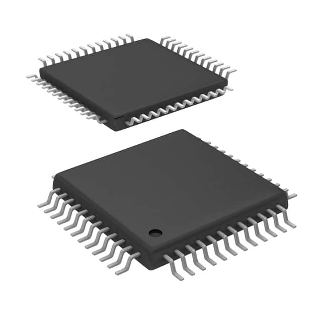
Texas Instruments TSB14AA1AIPFB
- Part No.:
- TSB14AA1AIPFB
- Manufacturer:
- Texas Instruments
- Category:
- Controllers
- Package:
- 48-TQFP
- Datasheet:
-
 TSB14AA1AIPFB.pdf
- Description:
- IC CONTROLLER ETHERNET 48TQFP
- Quantity:
- Payment:

- Shipping:

Inventory:1,343
Please send an inquiry. Send us your inquiry, and we will respond immediately.
Product details
Overview
TSB14AA1AIPFB from Texas Instruments is a 3.3-V IEEE 1394-1995/1394a-2000 backplane physical layer (PHY) transceiver for asynchronous-only operation at 50 or 100 Mbits/s. It provides LVCMOS-level PHY-link interface to link-layer controllers (e.g., TSB12LV01B), supports data-strobe bit-level encoding, and operates across 0°C to 70°C in a 48-pin TQFP (PFB) package. It requires external 49.152-MHz (S50) or 98.304-MHz (S100) oscillator input.
For engineers reviewing the TSB14AA1AIPFB datasheet, TSB14AA1AIPFB pinout, TSB14AA1AIPFB application, or TSB14AA1AIPFB equivalent, key selection considerations include its 3.3-V LVCMOS I/O compatibility, IEEE 1394a-compliant PHY-link timing, S50/S100 speed mode selection via CLK_SEL0/CLK_SEL1, support for 3-state or open-collector drivers, and requirement for external backplane driver circuitry.
Technical Context
The TSB14AA1AIPFB implements a dedicated backplane PHY layer with separate transmit (TDATA/TSTRB) and receive (RDATA/RSTRB) differential data-strobe paths. It performs real-time encoding/decoding of data-strobe streams, recovers clock from incoming strobe, and resynchronizes received data to the local system clock derived from an external oscillator.
It interfaces exclusively with IEEE 1394-compliant link-layer controllers via a parallel 2-bit-wide PHY-link bus. Clock generation is fully internal: the device divides the external reference (49.152 MHz or 98.304 MHz) to generate 24.576 MHz (S50) or 49.152 MHz (S100) system clocks for transmit/receive logic and LLC synchronization.
Key Specifications
| Parameter | Value and Actual Design Meaning |
|---|---|
| Supply Voltage | 3.3 V ±0.3 V - single-supply operation with 5-V-tolerant receive inputs |
| Data Rate | 50 or 100 Mbits/s asynchronous only - selectable via external oscillator and CLK_SEL pins |
| Operating Temperature | 0°C to 70°C - commercial grade, marked as 'I' suffix variant |
| Package | 48-pin TQFP (PFB), 7 mm × 7 mm × 1 mm - JEDEC-standard, RoHS-compliant, MSL Level-2 |
| PHY-Link Interface | Parallel 2-bit data/strobe bus - compliant with IEEE 1394a–2000 timing and register 0 auto-transfer on bus reset |
| Oscillator Input | 49.152 MHz (S50) or 98.304 MHz (S100) - externally supplied, not integrated |
| I/O Logic Level | LVCMOS - compatible with TI's TSB12LV-series link-layer controllers |
Pinout & Package
TSB14AA1AIPFB is housed in a 48-pin Plastic Quad Flatpack (TQFP-PFB), 7 mm × 7 mm body, 0.5 mm pitch, 1.2 mm max height, with exposed pad for thermal management per JEDEC MS-026.
| Pin/Terminal | Circuit Role | Design Meaning |
|---|---|---|
| VDD | Power supply | 3.3-V core and I/O supply; decoupling required per TI layout guidelines |
| GND | Ground reference | Common return for analog/digital sections; connect to exposed pad |
| TDATA, TSTRB | Transmit outputs | LVCMOS-encoded outbound data and strobe signals; require external backplane drivers |
| RDATA, RSTRB | Receive inputs | Differential data/strobe pair from backplane; 5-V tolerant |
| CLK_SEL0, CLK_SEL1 | Speed mode control | Binary-select S50 (00), S100 (01), or reserved modes; set at power-up |
| REFCLK | Oscillator input | Accepts 49.152 MHz (S50) or 98.304 MHz (S100) CMOS-level reference clock |
| PHY_RST#, PHY_CLK | Reset and clock output | Active-low asynchronous reset; 49.152-MHz clock output to LLC for synchronization |
| REG[7:0] | Configuration register bus | 8-bit parallel interface for read/write access to internal PHY registers per IEEE 1394a |
Key Features
| Feature | Design Value |
|---|---|
| IEEE 1394a–2000 PHY-link compliance | Guarantees interoperability with standard link-layer controllers including automatic register 0 transfer after bus reset |
| Data-strobe encoding/decoding | Enables robust clock recovery and bit-level synchronization without embedded clock in backplane signaling |
| External oscillator flexibility | Supports both S50 and S100 operation using industry-standard crystal frequencies (49.152/98.304 MHz) |
| 3-state and open-collector driver support | Allows direct interface to diverse backplane driver topologies without level-shifting or external logic |
| Extended register set with arbitration memory | Stores ID and priority of last arbitration-winning node, simplifying network initialization in multi-node backplanes |
Applications
| Backplane-Based Industrial Control Systems | High-Speed Test Equipment Backplanes |
|---|---|
Use Scenario: Multi-slot modular instrumentation chassis where modules exchange time-critical sensor data and control commands over a shared backplane. IC Role / Device Role / Timing Role: PHY layer transceiver handling physical signaling between slot-mounted nodes and central controller. Use Value: Enables deterministic 100-Mbit/s asynchronous transfers with low-latency clock recovery, supporting synchronized sampling across distributed modules. | Use Scenario: Automated test systems with plug-in measurement cards requiring hot-pluggable, self-identifying communication over a rigid backplane. IC Role / Device Role / Timing Role: Backplane PHY providing IEEE 1394a-compliant physical interface for card-to-backplane data exchange. Use Value: Delivers plug-and-play node enumeration and arbitration via built-in ID/priority storage, reducing firmware overhead during card insertion. |
| Medical Imaging Data Acquisition Chassis | Avionics Modular Processing Units |
Use Scenario: CT/MRI scanner front-end chassis aggregating high-fidelity analog-to-digital converter streams from multiple detector modules. IC Role / Device Role / Timing Role: Asynchronous PHY transceiver relaying encoded data-strobe frames from ADC modules to central processing unit. Use Value: Maintains signal integrity across long backplane traces using differential strobe-based clock recovery, eliminating skew-sensitive synchronous clock distribution. | Use Scenario: Ruggedized flight computer chassis with ARINC-653 partitioned modules exchanging health-monitoring and control packets. IC Role / Device Role / Timing Role: Deterministic backplane PHY enabling time-bounded packet delivery between safety-critical partitions. Use Value: Supports guaranteed 50-Mbit/s minimum throughput with IEEE 1394a arbitration, meeting DO-254 design assurance requirements for data path integrity. |
Equivalent & Alternatives
The following parts are listed as comparable options for similar IEEE 1394 backplane PHY applications.
| Alternative Part | Technical Difference | Application Difference | Selection Advice |
|---|---|---|---|
| TSB14AA1APFB | Same die, 0°C to 70°C commercial grade, identical pinout and electrical specs; differs only in marking and packaging (no 'I' suffix in part number) | No functional difference; used interchangeably where temperature range and traceability requirements align | Select TSB14AA1APFB if full TI part-number compliance without suffix notation is required for BOM standardization |
| TSB14C01APM | First-generation 1394 backplane PHY; lacks IEEE 1394a–2000 PHY-link compliance, smaller register set, no automatic register 0 transfer | Not suitable for new designs requiring 1394a arbitration enhancements or LLC interoperability with modern link-layer chips | Only consider TSB14C01APM for legacy repair or backward-compatible maintenance where 1394a features are unused |
Compared with TSB14AA1APFB, the TSB14AA1AIPFB offers identical functionality but with explicit 'I' temperature-grade marking and TI's G4 packaging revision; versus TSB14C01APM, it delivers mandatory 1394a PHY-link timing, expanded debug registers, and arbitration state retention-critical for reliable multi-node backplane initialization.
Availability
TSB14AA1AIPFB is available at Aetrix Electronics and suitable for backplane-based industrial control systems, high-speed test equipment chassis, and medical imaging data acquisition systems requiring stable component supply and long-term lifecycle support.
Supply support for TSB14AA1AIPFB includes scheduled delivery planning, volume procurement assistance, BOM continuity management, traceable sourcing, and lifecycle availability coordination for OEM customers, industrial embedded developers, connected-device designers, and electronics production programs.
Manufacturer
Texas Instruments is a global semiconductor company delivering analog and embedded processing solutions, with leadership in interface, timing, and connectivity technologies.
The TSB14AA1AIPFB belongs to TI's IEEE 1394 physical layer product line, designed specifically for high-reliability backplane implementations requiring deterministic asynchronous data transfer and seamless integration with 1394-compliant link-layer controllers.
FAQ
What is the operating temperature range specified for the TSB14AA1AIPFB?
The TSB14AA1AIPFB is rated for operation from 0°C to 70°C, as indicated by the 'I' suffix in its ordering code and confirmed in TI's Packaging Information Addendum. This commercial-grade temperature range is validated for continuous operation under stable ambient conditions and aligns with JEDEC JESD22-A104 reliability testing. The device does not support extended industrial or automotive temperature ranges; for those, alternate variants like TSB14AA1AT would be required. Always verify thermal derating in high-power-density PCB layouts.
Does the TSB14AA1AIPFB integrate an oscillator or require an external clock source?
The TSB14AA1AIPFB requires an external oscillator input - it does not contain an integrated crystal or PLL. It accepts either a 49.152-MHz signal for S50 operation or a 98.304-MHz signal for S100 operation on the REFCLK pin. These frequencies are divided internally to generate system clocks for encoding, decoding, and LLC synchronization. TI's SLLA222 datasheet specifies strict jitter and duty-cycle requirements for the external source to ensure compliant 1394 timing margins.
Can the TSB14AA1AIPFB drive a backplane directly without external components?
No, the TSB14AA1AIPFB cannot drive a backplane directly. Its TDATA and TSTRB outputs are LVCMOS-level signals intended for connection to external backplane drivers - either 3-state or open-collector types - as explicitly stated in the TI datasheet. The device lacks the current drive capability, termination control, or ESD robustness required for direct backplane connection. External drivers must provide proper impedance matching, slew rate control, and stub compensation per IEEE 1394 backplane specifications.
Which link-layer controllers are compatible with the TSB14AA1AIPFB?
The TSB14AA1AIPFB is designed to interface with TI's TSB12LV-series link-layer controllers, including the TSB12LV01B, TSB12LV32, and TSB12LV21B, as documented in the SLLA222 datasheet. Compatibility relies on strict adherence to the IEEE 1394a–2000 PHY-link timing specification, particularly for register access, bus reset response, and clock handoff via PHY_CLK. Non-TI LLCs must implement identical timing and register mapping to ensure interoperability.
What is the significance of the 'PFB' package designation in TSB14AA1AIPFB?
The 'PFB' in TSB14AA1AIPFB denotes Texas Instruments' standardized 48-pin Plastic Quad Flatpack (TQFP) package with 0.5-mm pitch, 7 mm × 7 mm body, and 1.2-mm maximum height - registered as JEDEC MS-026. It features an exposed thermal pad and is RoHS-compliant with NiPdAu (NIPDAU) lead finish and MSL Level-2 moisture sensitivity. This package enables high-density routing and thermal performance suitable for multi-layer backplane carrier boards, as verified in TI's PFB0048A mechanical drawing and board layout examples.
TSB14AA1AIPFB Specifications
- Product attributes
- Attribute value
- Manufacturer:
- Texas Instruments
- Package/Case:
- 48-TQFP
- Programmable:
- Not Verified
- Protocol:
- IEEE 1394
- Function:
- Physical Layer Controller
- Interface:
- -
- Standards:
- IEEE 1394-1995
- Voltage - Supply:
- 3.3V
- Current - Supply:
- -
- Operating Temperature:
- -40°C ~ 85°C
- Supplier Device Package:
- 48-TQFP (7x7)
- Grade:
- -
- Qualification:
- -
TSB14AA1AIPFB FAQ
1.How can I place an order for TSB14AA1AIPFB through Aetrix?
Please submit a Request for Quotation (RFQ) for TSB14AA1AIPFB on Aetrix. Our sales agent will provide a competitive quotation and guide you through the order confirmation once you accept the terms.
2.Are the price and stock information for TSB14AA1AIPFB reliable?
The price and inventory of TSB14AA1AIPFB are updated periodically and may fluctuate due to market conditions. Stock and pricing data are typically refreshed every 24 hours. Quotation validity for TSB14AA1AIPFB is usually 5 days.
3.What payment methods are accepted for TSB14AA1AIPFB?
We accept Wire Transfer, PayPal, Credit Card, Western Union, MoneyGram, and Escrow for TSB14AA1AIPFB transactions.
Note: Certain payment methods may incur a processing fee.
4.How is shipping managed for TSB14AA1AIPFB?
TSB14AA1AIPFB orders can be shipped via leading logistics carriers, including DHL, UPS, FedEx, TNT, or Registered Mail.
Once your TSB14AA1AIPFB order is processed, you will receive an email with the shipment details and tracking number.
Note: Tracking information may take up to 24 hours to appear. Express delivery typically takes 3–5 business days.
5.How can I obtain technical support or documentation for TSB14AA1AIPFB?
For technical support, including TSB14AA1AIPFB datasheets, pinout diagrams, or application guidance, please contact our engineering support team. They can provide detailed documentation and assistance for your TSB14AA1AIPFB requirements.
6.How does Aetrix verify that TSB14AA1AIPFB is sourced from the original manufacturer or authorized distributors?
All TSB14AA1AIPFB products on Aetrix are procured from qualified distributors and authorized channels. Our dedicated quality assurance team conducts strict verification, including traceability checks and, if necessary, third-party testing. This ensures that TSB14AA1AIPFB meets industry standards.
7.What is the process for return or replacement of TSB14AA1AIPFB?
All TSB14AA1AIPFB units undergo pre-shipment inspection (PSI). If there is an issue with TSB14AA1AIPFB, returns or replacements are accepted under the following conditions:
1.Quantity discrepancies, incorrect items, or visible external defects (such as breakage or corrosion), acknowledged by Aetrix.
2.The issue is reported within 90 days of delivery.
3.The TSB14AA1AIPFB part is unused and in its original packaging.
Return procedure for TSB14AA1AIPFB:
1.Submit a request within 90 days.
2.Obtain a Return Material Authorization (RMA) from Aetrix.
TSB14AA1AIPFB Tags

-
PTN5150AHXMP
NXP Semiconductors

-
USB3740B-AI9-TR
Microchip Technology

-
USB3740B-AI2-TR
Microchip Technology

-
USB3300-EZK-TR
Microchip Technology
-
USB3300-EZK
Microchip Technology

-
FUSB340TMX
onsemi

-
FUSB302BMPX
onsemi

-
DP83826IRHBR
Texas Instruments

-
MCP2518FDT-E/QBB
Microchip Technology
-
FUSB302MPX
onsemi

-
MCP2518FDT-E/SL
Microchip Technology

-
FT260Q-R
FTDI, Future Technology Devices International Ltd
Tech Hub

A practical engineering guide to 3.3V and 5V logic compatibility, input thresholds, resistor dividers, translator ICs, MOSFET level shifting, I2C pull-ups, timing limits and power-sequencing risks.

The 74HC595 uses push-pull logic outputs, while the TPIC6B595 uses 50 V open-drain DMOS sinks for higher-power loads. This guide compares timing, current limits, 3.3 V interfacing, load wiring, thermal…

The 74HC595 converts serial data into eight stable parallel outputs. This guide covers pin functions, shift and storage timing, OE and MR behavior, drive-current limits, cascading, voltage compatibilit…

A technical comparison of level-sensitive latches and edge-triggered flip-flops, covering timing windows, setup and hold limits, master–slave operation, time borrowing, race-through, HDL inference and…

A D latch stores one bit while Enable controls when data can pass. This reference covers gate-level operation, truth tables, transparency, setup and hold timing, LE versus OE, common ICs and practical …

An SR latch stores one bit through cross-coupled feedback. This engineering reference covers NOR and NAND implementations, truth tables, forbidden-state recovery, gated operation, switch debouncing, fa…

Latch circuits retain one bit through feedback. This technical reference covers SR and D latches, truth tables, transparency, timing limits, latch-versus-flip-flop behavior, applications and common log…

An engineering guide to LED driver operation, constant-current and constant-voltage outputs, linear and switching topologies, dimming, IC selection, calculations, replacement compatibility, and fault c…

Operational amplifier guide covering op amp basics, feedback, ideal vs real op amps, common configurations, buffer circuits, offset, bias current, gain-bandwidth, slew rate, rail-to-rail limits and sel…

Jumper cables guide covering safe connection order, red and black clamp placement, final ground connection, cable gauge, length, clamp quality, copper vs CCA cables, jump starter comparison and battery…


