
 My Inquiry
 My Account


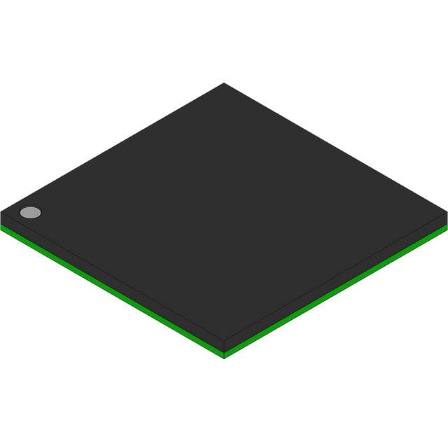
Texas Instruments TSB43AA82IGGW
- Part No.:
- TSB43AA82IGGW
- Manufacturer:
- Texas Instruments
- Category:
- Controllers
- Package:
- -
- Datasheet:
-
 TSB43AA82IGGW.pdf
- Description:
- SERIAL I/O CONTROLLER
- Quantity:
- Payment:

- Shipping:

Inventory:254
Please send an inquiry. Send us your inquiry, and we will respond immediately.
Product details
Overview
TSB43AA82IGGW from Texas Instruments is an IEEE 1394a-2000–compliant integrated PHY and link-layer controller for SBP-2 and DPP applications. It features dual 400-Mbps 1394 ports, 3.3-V supply with internal 1.8-V regulation, 176-pin BGA (GGW) industrial-grade packaging (–40°C to 85°C), and three independent FIFOs: 1512-byte async command, 4728-byte DMA, and 504-byte Config ROM/LOG.
For engineers reviewing the TSB43AA82IGGW datasheet, TSB43AA82IGGW pinout, TSB43AA82IGGW application, or TSB43AA82IGGW equivalent, key selection criteria include IEEE 1394a compliance, industrial temperature range, SBP-2 transaction automation (ORB/page table fetch), ATAPI/SCSI mode support, and dual-port BGA implementation for high-volume CE storage peripherals.
Technical Context
The TSB43AA82IGGW integrates a two-port 400-Mbps physical layer and full link-layer controller in a single die, enabling direct connection to host microcontrollers via 8-/16-bit asynchronous/synchronous or multiplexed bus interfaces up to 40 MHz. It implements automated IEEE 1394 configuration ROM read responses and split-transaction retry control via configurable time-limit registers.
Its SBP-2 engine supports up to four initiators with fully automated ORB fetching, linked-command handling, and page-table management-eliminating firmware overhead for SCSI-over-1394 storage bridging. The DPP mode leverages the asynchronous receive FIFO as a segment data unit register for large print-data transfers.
Key Specifications
| Parameter | Value and Actual Design Meaning |
|---|---|
| IEEE Compliance | IEEE 1394a-2000 and IEEE 1394-1995 - ensures interoperability with legacy and enhanced FireWire devices including arbitration, isochronous/asynchronous timing, and PHY layer signaling. |
| Data Rate | 400 Mbps per port - enables high-bandwidth storage bridging (e.g., external HDD enclosures) without bottlenecking ATAPI Ultra-DMA or SCSI command throughput. |
| Supply Voltage | Single 3.3-V supply with internal 1.8-V regulator - reduces external power design complexity and lowers active power consumption in CE systems. |
| FIFO Allocation | Async Command: 1512 B; DMA: 4728 B; Config ROM/LOG: 504 B - provides dedicated, non-blocking buffers for concurrent command parsing, bulk data transfer, and device identification. |
| Host Interface | 8-/16-bit async/sync or multiplexed bus, up to 40 MHz - supports direct attachment to common MCUs (e.g., ARM7, MIPS-based controllers) without glue logic or clock domain translation. |
| Operating Temperature | –40°C to +85°C - qualifies for industrial-grade embedded storage subsystems where ambient thermal stability exceeds commercial-grade limits. |
Pinout & Package
TSB43AA82IGGW uses a 176-terminal microstar BGA (GGW) package with 0.8-mm ball pitch, 13.5 mm × 13.5 mm body size, and JEDEC-standard moisture sensitivity level (MSL) rating. Pinout is defined in TI SLLA204 (Rev. JUNE 2006), Section 5 "Signal Descriptions" and Figure 5–1 "Pin Assignments".
| Pin/Terminal | Circuit Role | Design Meaning |
|---|---|---|
| CLKIN | Reference Clock Input | Accepts 24.576-MHz crystal or oscillator input to synchronize 1394 PHY timing and internal state machines. |
| RESET# | Active-Low Reset | Asynchronous hardware reset that clears all internal registers and forces reinitialization of link negotiation and configuration ROM access. |
| AS# / DS# | Address Strobe / Data Strobe | Controls 8-/16-bit host bus timing: AS# enables address latching; DS# enables data capture during read/write cycles. |
| INT# | Interrupt Output | Open-drain active-low signal indicating completion of DMA transfers, ORB processing, or error conditions requiring host attention. |
| TPA+/TPA− TPB+/TPB− | Dual 1394 Port Differential Pairs | Two independent twisted-pair transceiver interfaces supporting full-duplex 1394 cable connectivity with automatic speed negotiation (100/200/400 Mbps). |
Key Features
| Feature | Design Value |
|---|---|
| Automated ORB Fetching | Hardware-accelerated retrieval of operation request blocks from host memory eliminates CPU polling and reduces firmware latency in SBP-2 storage stacks. |
| Config ROM Read Response | On-chip logic automatically responds to remote node Config ROM reads - no host intervention required for IEEE 1394 self-identification and topology discovery. |
| Split Transaction Control | Programmable timeout and single-retry protocol enforcement via CFR register - ensures deterministic response timing for legacy 1394 devices with limited buffer resources. |
| ATAPI/SCSI Mode Support | Native command mapping and status reporting for both ATAPI Ultra-DMA and SCSI protocols - enables single-chip bridging between 1394 and parallel storage interfaces. |
| DPP Segment Data Unit Mode | ARF repurposed as SDU register - allows large print-job payloads to be segmented and transmitted over 1394 without host-side buffering or fragmentation logic. |
Applications
| External Hard Drive Enclosure | Digital Camcorder Interface Bridge |
|---|---|
Use Scenario: High-speed connection of 2.5″ SATA HDDs to desktop/laptop PCs via FireWire 400. IC Role / Device Role / Timing Role: Dual-port 1394 PHY + link-layer controller managing isochronous video streaming and asynchronous command/data transfers between host and drive. Use Value: Enables plug-and-play storage with guaranteed 400-Mbps bandwidth, automated SBP-2 ORB execution, and industrial temp resilience for portable enclosures. | Use Scenario: Real-time bidirectional transfer of DV-format video streams between camcorders and editing workstations. IC Role / Device Role / Timing Role: IEEE 1394a-compliant interface bridge converting parallel DV data to serial 1394 packets with precise isochronous timing and cycle master arbitration. Use Value: Delivers sub-frame jitter-free video transport using hardware-managed isochronous resource allocation and auto-negotiated 400-Mbps link speed. |
| Network-Attached Storage Adapter | Direct Print Protocol (DPP) Printer Controller |
Use Scenario: Embedded NAS gateway connecting multiple USB/SATA drives to FireWire-equipped Macintosh or Linux hosts. IC Role / Device Role / Timing Role: Link-layer controller handling concurrent SBP-2 initiator sessions (up to four) with automated page-table fetches for scatter-gather I/O. Use Value: Supports multi-drive RAID configurations with zero-host CPU overhead for command queuing and memory-mapped buffer management. | Use Scenario: High-volume office printer supporting FireWire-connected host PCs for direct print job submission without USB or Ethernet. IC Role / Device Role / Timing Role: DPP-mode controller using ARF as SDU register to receive segmented print data and manage end-to-end flow control with ACK/NACK signaling. Use Value: Eliminates need for external print-spool RAM and enables native FireWire print driver integration with deterministic large-payload delivery. |
Equivalent & Alternatives
The following parts are listed as comparable options for similar 1394 link-layer controller applications.
| Alternative Part | Technical Difference | Application Difference | Selection Advice |
|---|---|---|---|
| TSB43AA82GGW | Commercial temperature grade (0°C to 70°C); identical GGW BGA package, pinout, and functional spec. | Limited to indoor, climate-controlled CE environments; not rated for extended thermal cycling or industrial chassis mounting. | Select when cost-sensitive consumer electronics require same footprint and firmware compatibility but relaxed environmental specs. |
| TSB43AA82PGE | 144-pin LQFP package; same core functionality but different mechanical layout, thermal profile, and board-level routing requirements. | Preferred for prototyping, low-volume industrial designs, or space-constrained layouts where BGA rework is impractical. | Choose when manual assembly, test accessibility, or thermal pad soldering constraints make BGA unsuitable despite identical electrical behavior. |
Compared with TSB43AA82IGGW, the TSB43AA82GGW offers identical performance at lower cost but lacks industrial temperature resilience, while the TSB43AA82PGE provides equivalent functionality in a rework-friendly LQFP-enabling faster validation and simplified thermal management at the expense of board area and signal integrity margin.
Availability
TSB43AA82IGGW is available at Aetrix Electronics and suitable for external hard drive enclosures, digital camcorder bridges, network-attached storage adapters, and Direct Print Protocol printer controllers requiring stable component supply across industrial temperature ranges and long production lifecycles.
Supply support for TSB43AA82IGGW includes scheduled delivery planning, volume procurement assistance, BOM continuity management, traceable sourcing, and lifecycle availability coordination for OEM customers, industrial embedded developers, connected-device designers, and electronics production programs.
Manufacturer
Texas Instruments is a global semiconductor company headquartered in Dallas, Texas, delivering analog and embedded processing solutions for industrial, automotive, personal electronics, and communications markets.
The TSB43AA82IGGW belongs to TI's IEEE 1394 interface product line, engineered specifically for high-volume consumer electronics requiring certified FireWire 400 connectivity with minimal host processor overhead and robust SBP-2/DPP protocol acceleration.
FAQ
What is the operating temperature range of the TSB43AA82IGGW?
The TSB43AA82IGGW is rated for industrial operation from –40°C to +85°C. This extended range is achieved through process and packaging optimizations validated per TI's qualification standards and distinguishes it from the commercial-grade TSB43AA82GGW. The TSB43AA82IGGW maintains full IEEE 1394a-2000 compliance and FIFO performance across this entire range without derating.
Does the TSB43AA82IGGW support both SBP-2 and DPP protocols simultaneously?
Yes, the TSB43AA82IGGW supports SBP-2 and DPP concurrently via separate hardware engines. Its SBP-2 transaction manager handles up to four initiators with automated ORB and page-table fetching, while its DPP mode repurposes the asynchronous receive FIFO as a segment data unit register. Both protocols operate independently under shared 1394 PHY resources without conflict or firmware arbitration.
Is the TSB43AA82IGGW pin-compatible with other variants in the TSB43AA82 family?
The TSB43AA82IGGW shares identical pinout and ball assignment with the TSB43AA82GGW (same GGW BGA package), making them mechanically and electrically interchangeable on PCBs designed for either variant. However, it is not pin-compatible with the TSB43AA82PGE (144-pin LQFP), which uses a completely different footprint, pad layout, and thermal pad configuration.
What host bus interface modes does the TSB43AA82IGGW support?
The TSB43AA82IGGW supports three host bus configurations: 8-bit or 16-bit asynchronous, 8-bit or 16-bit synchronous, and 8-bit or 16-bit multiplexed address/data. All modes operate up to 40 MHz and interface directly to standard microcontrollers without external wait-state generators or bus translators. The TSB43AA82IGGW's AS#/DS# and RD#/WR# signals provide precise timing control for each mode.
How does the TSB43AA82IGGW handle IEEE 1394 configuration ROM access?
The TSB43AA82IGGW implements fully automated configuration ROM read responses in hardware. When a remote node issues a read request to the Config ROM address space, the TSB43AA82IGGW retrieves the stored ROM image from its internal 504-byte Config ROM/LOG FIFO and returns valid data without host CPU involvement. This feature is mandatory for IEEE 1394 self-identification and topology enumeration.
TSB43AA82IGGW Specifications
- Product attributes
- Attribute value
- Manufacturer:
- Texas Instruments
- Package/Case:
- -
- Programmable:
- Not Verified
- Protocol:
- -
- Function:
- -
- Interface:
- -
- Standards:
- -
- Voltage - Supply:
- -
- Current - Supply:
- -
- Operating Temperature:
- -
- Supplier Device Package:
- -
- Grade:
- -
- Qualification:
- -
TSB43AA82IGGW FAQ
1.How can I place an order for TSB43AA82IGGW through Aetrix?
Please submit a Request for Quotation (RFQ) for TSB43AA82IGGW on Aetrix. Our sales agent will provide a competitive quotation and guide you through the order confirmation once you accept the terms.
2.Are the price and stock information for TSB43AA82IGGW reliable?
The price and inventory of TSB43AA82IGGW are updated periodically and may fluctuate due to market conditions. Stock and pricing data are typically refreshed every 24 hours. Quotation validity for TSB43AA82IGGW is usually 5 days.
3.What payment methods are accepted for TSB43AA82IGGW?
We accept Wire Transfer, PayPal, Credit Card, Western Union, MoneyGram, and Escrow for TSB43AA82IGGW transactions.
Note: Certain payment methods may incur a processing fee.
4.How is shipping managed for TSB43AA82IGGW?
TSB43AA82IGGW orders can be shipped via leading logistics carriers, including DHL, UPS, FedEx, TNT, or Registered Mail.
Once your TSB43AA82IGGW order is processed, you will receive an email with the shipment details and tracking number.
Note: Tracking information may take up to 24 hours to appear. Express delivery typically takes 3–5 business days.
5.How can I obtain technical support or documentation for TSB43AA82IGGW?
For technical support, including TSB43AA82IGGW datasheets, pinout diagrams, or application guidance, please contact our engineering support team. They can provide detailed documentation and assistance for your TSB43AA82IGGW requirements.
6.How does Aetrix verify that TSB43AA82IGGW is sourced from the original manufacturer or authorized distributors?
All TSB43AA82IGGW products on Aetrix are procured from qualified distributors and authorized channels. Our dedicated quality assurance team conducts strict verification, including traceability checks and, if necessary, third-party testing. This ensures that TSB43AA82IGGW meets industry standards.
7.What is the process for return or replacement of TSB43AA82IGGW?
All TSB43AA82IGGW units undergo pre-shipment inspection (PSI). If there is an issue with TSB43AA82IGGW, returns or replacements are accepted under the following conditions:
1.Quantity discrepancies, incorrect items, or visible external defects (such as breakage or corrosion), acknowledged by Aetrix.
2.The issue is reported within 90 days of delivery.
3.The TSB43AA82IGGW part is unused and in its original packaging.
Return procedure for TSB43AA82IGGW:
1.Submit a request within 90 days.
2.Obtain a Return Material Authorization (RMA) from Aetrix.
TSB43AA82IGGW Tags

-
PTN5150AHXMP
NXP Semiconductors

-
USB3740B-AI9-TR
Microchip Technology

-
USB3740B-AI2-TR
Microchip Technology

-
USB3300-EZK-TR
Microchip Technology
-
USB3300-EZK
Microchip Technology

-
FUSB340TMX
onsemi

-
FUSB302BMPX
onsemi

-
DP83826IRHBR
Texas Instruments

-
MCP2518FDT-E/QBB
Microchip Technology
-
FUSB302MPX
onsemi

-
MCP2518FDT-E/SL
Microchip Technology

-
FT260Q-R
FTDI, Future Technology Devices International Ltd
Tech Hub

A practical engineering guide to 3.3V and 5V logic compatibility, input thresholds, resistor dividers, translator ICs, MOSFET level shifting, I2C pull-ups, timing limits and power-sequencing risks.

The 74HC595 uses push-pull logic outputs, while the TPIC6B595 uses 50 V open-drain DMOS sinks for higher-power loads. This guide compares timing, current limits, 3.3 V interfacing, load wiring, thermal…

The 74HC595 converts serial data into eight stable parallel outputs. This guide covers pin functions, shift and storage timing, OE and MR behavior, drive-current limits, cascading, voltage compatibilit…

A technical comparison of level-sensitive latches and edge-triggered flip-flops, covering timing windows, setup and hold limits, master–slave operation, time borrowing, race-through, HDL inference and…

A D latch stores one bit while Enable controls when data can pass. This reference covers gate-level operation, truth tables, transparency, setup and hold timing, LE versus OE, common ICs and practical …

An SR latch stores one bit through cross-coupled feedback. This engineering reference covers NOR and NAND implementations, truth tables, forbidden-state recovery, gated operation, switch debouncing, fa…

Latch circuits retain one bit through feedback. This technical reference covers SR and D latches, truth tables, transparency, timing limits, latch-versus-flip-flop behavior, applications and common log…

An engineering guide to LED driver operation, constant-current and constant-voltage outputs, linear and switching topologies, dimming, IC selection, calculations, replacement compatibility, and fault c…

Operational amplifier guide covering op amp basics, feedback, ideal vs real op amps, common configurations, buffer circuits, offset, bias current, gain-bandwidth, slew rate, rail-to-rail limits and sel…

Jumper cables guide covering safe connection order, red and black clamp placement, final ground connection, cable gauge, length, clamp quality, copper vs CCA cables, jump starter comparison and battery…


